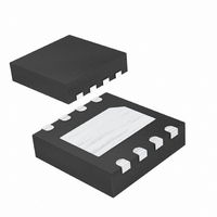
MAX1288ETA+T Maxim Integrated Products, MAX1288ETA+T Datasheet

MAX1288ETA+T
Specifications of MAX1288ETA+T
Related parts for MAX1288ETA+T
MAX1288ETA+T Summary of contents
Page 1
... SPI-/QSPI-/MICROWIRE-Compatible Interface for DSPs and Processors o Internal Conversion Clock o 8-Pin SOT23 and 8-Pin TDFN Packages Applications PART MAX1286EKA-T MAX1286ETA+T MAX1287EKA-T MAX1287ETA+T MAX1288EKA-T MAX1288ETA+T MAX1289EKA-T MAX1289ETA Note: All devices specified over the -40°C to +85°C operating range . + Denotes a lead(Pb)-free/RoHS-compliant package . MAX1286– ...
Page 2
Single-Ended, and 1-Channel True-Differential ADCs ABSOLUTE MAXIMUM RATINGS V to GND ..............................................................-0.3V to +6V DD CNVST, SCLK, DOUT to GND....................-0. REF, AIN1 (AIN+), AIN2 (AIN-) to GND......-0. Maximum Current into Any Pin............................................50mA Continuous ...
Page 3
Single-Ended, and ELECTRICAL CHARACTERISTICS (continued +2.7V to +3.6V +2.5V for MAX1287/MAX1289 REF 0.1µF capacitor at REF 8MHz (50% duty cycle), AIN- = GND for MAX1288/MAX1289. T SCLK noted. ...
Page 4
Single-Ended, and 1-Channel True-Differential ADCs TIMING CHARACTERISTICS (Figures 1, 2, and +2.7V to +3.6V +2.5V, 0.1µF capacitor at REF REF 0.1µF capacitor at REF 8MHz (50% duty ...
Page 5
Single-Ended, and (V = +3V +2.5V for MAX1287/MAX1289 REF f = 8MHz (50% duty cycle); AIN- = GND for MAX1288/MAX1289, T SCLK INTEGRAL NONLINEARITY vs. OUTPUT CODE 1.0 MAX1287/MAX1289 0.8 0.6 0.4 0.2 ...
Page 6
Single-Ended, and 1-Channel True-Differential ADCs (V = +3V +2.5V for MAX1287/MAX1284 REF f = 8MHz (50% duty cycle); AIN- = GND for MAX1288/MAX1289, T SCLK SHUTDOWN CURRENT vs. TEMPERATURE 300 250 200 150 ...
Page 7
Single-Ended, and NAME PIN MAX1286 MAX1288 MAX1287 MAX1289 Positive Supply Voltage. +2.7V to +3.6V (MAX1287/MAX1289); +4.75V to +5.25V (MAX1286/MAX1288). Bypass with a 0.1µF capacitor to GND. 2 AIN1 AIN+ Analog Input Channel ...
Page 8
Single-Ended, and 1-Channel True-Differential ADCs REF DAC AIN2 GND AIN1 (AIN+) CIN+ HOLD CIN- RIN- GND (AIN-) HOLD TRACK ARE FOR MAX1288/MAX1289 Figure 4. Equivalent Input Circuit where R = 1.5kΩ, R ...
Page 9
Single-Ended, and t CONV t ACQ CNVST 1 SCLK B11 DOUT MSB HIGH-Z SAMPLING INSTANT Figure 5a. Single Conversion AIN1 vs. GND (MAX1286/MAX1287), Unipolar Mode AIN+ vs. AIN- (MAX1288/MAX1289) t CONV t ACQ CNVST 1 SCLK B11 ...
Page 10
Single-Ended, and 1-Channel True-Differential ADCs Output Data Format Figures 5a and 5b illustrate the conversion timing for the MAX1286–MAX1289. The 12-bit conversion result is out- put in MSB-first format. Data on DOUT transitions on the falling edge ...
Page 11
Single-Ended, and 5) Activate SCLK for a minimum of 12 rising clock edges. DOUT transitions on SCLK’s falling edge and is available in MSB-first format. Observe the SCLK to DOUT valid timing characteristic. Clock data into the ...
Page 12
Single-Ended, and 1-Channel True-Differential ADCs CNVST 1ST BYTE READ 1 SCLK B11 DOUT B10 B9 B8 MSB SAMPLING INSTANT Figure 8c. SPI/MICROWIRE Interface Timing Sequence (CPOL = CPHA = 0) Layout, Grounding, and Bypassing For best performance, ...
Page 13
Single-Ended, and CNVST 1 SCLK B11 DOUT B10 B9 MSB SAMPLING INSTANT Figure 9b. QSPI Interface Timing Sequence (CPOL = CPHA = SCLK DOUT CNVST MAX1286– MAX1289 GND Figure 10a. SPI Interface Connection for ...
Page 14
Single-Ended, and 1-Channel True-Differential ADCs SUPPLIES + 5Ω 0.1µF GND V DD MAX1286– MAX1289 *OPTIONAL Figure 11. Power-Supply and Grounding Connections Aperture Definitions Aperture jitter ( the sample-to-sample variation in AJ ...
Page 15
... Maxim cannot assume responsibility for use of any circuitry other than circuitry entirely embodied in a Maxim product. No circuit patent licenses are implied. Maxim reserves the right to change the circuitry and specifications without notice at any time. Maxim Integrated Products, 120 San Gabriel Drive, Sunnyvale, CA 94086 408-737-7600 ____________________ 15 © 2010 Maxim Integrated Products ...


