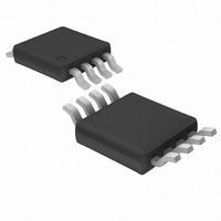
LTC1860CMS8#TR Linear Technology, LTC1860CMS8#TR Datasheet

LTC1860CMS8#TR
Specifications of LTC1860CMS8#TR
Available stocks
Related parts for LTC1860CMS8#TR
LTC1860CMS8#TR Summary of contents
Page 1
... LT, LTC and LTM are registered trademarks of Linear Technology Corporation. All other trademarks are the property of their respective owners. Supply Current vs Sampling Frequency 1000 ...
Page 2
LTC1860/LTC1861 ABSOLUTE MAXIMUM RATINGS (Notes 1, 2) Supply Voltage (V ) .................................................7V CC Ground Voltage Difference AGND, DGND LTC1861 MSOP Package .............±0.3V Analog Input ....................(GND – 0.3V Digital Input .................................... (GND – 0.3V Digital Output ................... ...
Page 3
... ORDER INFORMATION LEAD FREE FINISH TAPE AND REEL LTC1860CMS8#PBF LTC1860CMS8#TRPBF LTC1860IMS8#PBF LTC1860IMS8#PBF LTC1860HMS8#PBF LTC1860HMS8#PBF LTC1860CS8#PBF LTC1860CS8#PBF LTC1860IS8#PBF LTC1860IS8#PBF LTC1861CMS#PBF LTC1861CMS#PBF LTC1861IMS#PBF LTC1861IMS#PBF LTC1861HMS#PBF LTC1861HMS#PBF LTC1861CS8#PBF LTC1861CS8#PBF LTC1861IS8#PBF LTC1861IS8#PBF LEAD BASED FINISH TAPE AND REEL LTC1860CMS8 LTC1860CMS8 LTC1860IMS8 LTC1860IMS8 LTC1860HMS8 LTC1860HMS8 LTC1860CS8 ...
Page 4
LTC1860/LTC1861 CONVERTER AND MULTIPLEXER CHARACTERISTICS The ● denotes specifi cations which apply over the full operating temperature range, otherwise specifi cations are 5V 5V defi ned in Recommended Operating Conditions, unless ...
Page 5
DIGITAL AND DC ELECTRICAL CHARACTERISTICS over the full operating temperature range, otherwise specifi cations are T SYMBOL PARAMETER I Hi-Z Output Leakage OZ I Output Source Current SOURCE I Output Sink Current SINK I Reference Current (LTC1860 SO-8, REF MSOP ...
Page 6
LTC1860/LTC1861 TIMING CHARACTERISTICS range, otherwise specifi cations are T A Conditions, unless otherwise noted. SYMBOL PARAMETER t Conversion Time (See Figure 1) CONV f Maximum Sampling Frequency SMPL(MAX) t Delay Time, SCK↓ to SDO Data Valid dDO t Delay Time, ...
Page 7
TYPICAL PERFORMANCE CHARACTERISTICS Supply Current vs Sampling Frequency 1000 CONV LOW = 800ns 100 0.1 0.01 0.01 0.1 1.0 10 100 1000 SAMPLING FREQUENCY (kHz) 1860/61 G01 Reference Current ...
Page 8
LTC1860/LTC1861 TYPICAL PERFORMANCE CHARACTERISTICS Change in Offset Error vs Reference Voltage –1 –2 –3 –4 – REFERENCE VOLTAGE (V) 1860/61 ...
Page 9
PIN FUNCTIONS LTC1860 V (Pin 1): Reference Input. The reference input defi nes REF the span of the A/D converter and must be kept free of noise with respect to GND. + – (Pins 2, 3): Analog ...
Page 10
LTC1860/LTC1861 FUNCTIONAL BLOCK DIAGRAM PIN NAMES IN PARENTHESES REFER TO LTC1861 + IN (CH0) – IN (CH1) GND TEST CIRCUITS Load Circuit for dDO r f TEST POINT V 3k SDO t 20pF ...
Page 11
APPLICATIONS INFORMATION CONV t CONV SCK SDO • • • ...
Page 12
LTC1860/LTC1861 APPLICATIONS INFORMATION CONV t CONV SDI SCK SDO • • • ...
Page 13
APPLICATIONS INFORMATION Reference Input The reference input of the LTC1861 SO-8 package is internally tied The span of the A/D converter is CC therefore equal The voltage on the reference input CC of the ...
Page 14
LTC1860/LTC1861 PACKAGE DESCRIPTION 0.889 0.127 (.035 .005) 5.23 3.20 – 3.45 (.206) (.126 – .136) MIN 0.42 0.038 0.65 (.0256) (.0165 .0015) TYP BSC RECOMMENDED SOLDER PAD LAYOUT NOTE: 1. DIMENSIONS IN MILLIMETER/(INCH) 2. DRAWING NOT TO SCALE 3. DIMENSION ...
Page 15
... MOLD FLASH OR PROTRUSIONS SHALL NOT EXCEED .006" (0.15mm) Information furnished by Linear Technology Corporation is believed to be accurate and reliable. However, no responsibility is assumed for its use. Linear Technology Corporation makes no representa- tion that the interconnection of its circuits as described herein will not infringe on existing patent rights. ...
Page 16
... SO-8, MS8, 1-Channel, 5V/SO-8, MS10, 2-Channel, 5V Bandgap, 130μA Supply Current, 10ppm/°C, Available in SOT-23 60μA Supply Current, 10ppm/°C, SOT-23 www.linear.com ● 4.096V 0 REF 0 REF 7 SCK 6 SDO 5 CONV GND 4 1860 TA03 LT 1207 REV A • PRINTED IN USA © LINEAR TECHNOLOGY CORPORATION 2007 18601fa ...


