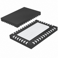
LTC2449CUHF Linear Technology, LTC2449CUHF Datasheet - Page 11

LTC2449CUHF
Manufacturer Part Number
LTC2449CUHF
Description
IC ADC 24BIT HI SPEED 38QFN
Manufacturer
Linear Technology
Datasheet
1.LTC2445CUHFPBF.pdf
(28 pages)
Specifications of LTC2449CUHF
Number Of Bits
24
Sampling Rate (per Second)
8k
Data Interface
MICROWIRE™, Serial, SPI™
Number Of Converters
1
Power Dissipation (max)
40mW
Voltage Supply Source
Single Supply
Operating Temperature
0°C ~ 70°C
Mounting Type
Surface Mount
Package / Case
38-WFQFN, Exposed Pad
Lead Free Status / RoHS Status
Contains lead / RoHS non-compliant
Available stocks
Company
Part Number
Manufacturer
Quantity
Price
Company:
Part Number:
LTC2449CUHF
Manufacturer:
LT
Quantity:
10 000
Part Number:
LTC2449CUHF
Manufacturer:
LINEAR/凌特
Quantity:
20 000
Part Number:
LTC2449CUHF#PBF
Manufacturer:
LINEAR/凌特
Quantity:
20 000
Part Number:
LTC2449CUHF#TRPBF
Manufacturer:
LINEAR/凌特
Quantity:
20 000
APPLICATIO S I FOR ATIO
external SCK mode is selected by tying EXT (Pin 3) LOW
for external SCK and HIGH for internal SCK.
Serial Data Output (SDO)
The serial data output pin, SDO (Pin 37), provides the
result of the last conversion as a serial bit stream (MSB
first) during the data output state. In addition, the SDO pin
is used as an end of conversion indicator during the
conversion and sleep states.
When CS (Pin 36) is HIGH, the SDO driver is switched to
a high impedance state. This allows sharing the serial
interface with other devices. If CS is LOW during the
convert or sleep state, SDO will output EOC. If CS is LOW
during the conversion phase, the EOC bit appears HIGH on
the SDO pin. Once the conversion is complete, EOC goes
LOW. The device remains in the sleep state until the first
rising edge of SCK occurs while CS = LOW.
Chip Select Input (CS)
The active LOW chip select, CS (Pin 36), is used to test the
conversion status and to enable the data output transfer as
described in the previous sections.
In addition, the CS signal can be used to trigger a new
conversion cycle before the entire serial data transfer has
been completed. The LTC2444/LTC2445/LTC2448/
LTC2449 will abort any serial data transfer in progress and
start a new conversion cycle anytime a LOW-to-HIGH
transition is detected at the CS pin after the converter has
entered the data output state.
Serial Data Input (SDI)
The serial data input (SDI, Pin 34) is used to select the
speed/resolution and input channel of the LTC2444/
LTC2445/LTC2448/LTC2449. SDI is programmed by a
serial input data stream under the control of SCK during
the data output cycle, see Figure 3.
Initially, after powering up, the device performs a conver-
sion with IN
+
= CH0, IN
U
–
= CH1, OSR = 256 (output rate
U
W
U
nominally 880Hz), and 1X speedup mode (no Latency).
Once this first conversion is complete, the device enters
the sleep state and is ready to output the conversion result
and receive the serial data input stream programming the
speed/resolution and input channel for the next conver-
sion. At the conclusion of each conversion cycle, the
device enters this state.
In order to change the speed/resolution or input channel,
the first 3 bits shifted into the device are 101. This is
compatible with the programming sequence of the
LTC2414/LTC2418. If the sequence is set to 000 or 100,
the following input data is ignored (don’t care) and the
previously selected speed/resolution and channel remain
valid for the next conversion. Combinations other than
101, 100, and 000 of the 3 control bits should be avoided.
If the first 3 bits shifted into the device are 101, then the
following 5 bits select the input channel for the following
conversion (see Tables 3 and 4). The next 5 bits select the
speed/resolution and mode 1X (no Latency) 2X (double
output rate with one conversion latency), see Table 5. If
these 5 bits are set to all 0’s, the previous speed remains
selected for the next conversion. This is useful in applica-
tions requiring a fixed output rate/resolution but need to
change the input channel. In this case, the timing and input
sequence is compatible with the LTC2414/LTC2418.
When an update operation is initiated (the first 3 bits are
101) the first 5 bits are the channel address. The first
bit, SGL, determines if the input selection is differential
(SGL = 0) or single-ended (SGL = 1). For SGL = 0, two
adjacent channels can be selected to form a differential
input. For SGL = 1, one of 8 channels (LTC2444/LTC2445)
or one of 16 channels (LTC2448/LTC2449) is selected as
the positive input. The negative input is COM for all single
ended operations. The remaining 4 bits (ODD, A2, A1, A0)
determine which channel is selected. The LTC2448/
LTC2449 use all 4 bits to select one of 16 different input
channels (see table 3) while in the case of the LTC2444/
LTC2445, A2 is always 0, and the remaining 3 bits select
one of 8 different input channels (see Table 4).
LTC2444/LTC2445/
LTC2448/LTC2449
11
2444589fb


