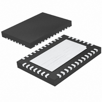
LTC2449CUHF Linear Technology, LTC2449CUHF Datasheet - Page 18

LTC2449CUHF
Manufacturer Part Number
LTC2449CUHF
Description
IC ADC 24BIT HI SPEED 38QFN
Manufacturer
Linear Technology
Datasheet
1.LTC2445CUHFPBF.pdf
(28 pages)
Specifications of LTC2449CUHF
Number Of Bits
24
Sampling Rate (per Second)
8k
Data Interface
MICROWIRE™, Serial, SPI™
Number Of Converters
1
Power Dissipation (max)
40mW
Voltage Supply Source
Single Supply
Operating Temperature
0°C ~ 70°C
Mounting Type
Surface Mount
Package / Case
38-WFQFN, Exposed Pad
Lead Free Status / RoHS Status
Contains lead / RoHS non-compliant
Available stocks
Company
Part Number
Manufacturer
Quantity
Price
Company:
Part Number:
LTC2449CUHF
Manufacturer:
LT
Quantity:
10 000
Part Number:
LTC2449CUHF
Manufacturer:
LINEAR/凌特
Quantity:
20 000
Part Number:
LTC2449CUHF#PBF
Manufacturer:
LINEAR/凌特
Quantity:
20 000
Part Number:
LTC2449CUHF#TRPBF
Manufacturer:
LINEAR/凌特
Quantity:
20 000
APPLICATIO S I FOR ATIO
LTC2444/LTC2445/
LTC2448/LTC2449
External Serial Clock, 2-Wire I/O
This timing mode utilizes a 2-wire serial I/O interface. The
conversion result is shifted out of the device by an exter-
nally generated serial clock (SCK) signal, see Figure 6. CS
may be permanently tied to ground, simplifying the user
interface or isolation barrier. The external serial clock
mode is selected by tying EXT LOW.
Since CS is tied LOW, the end-of-conversion (EOC) can be
continuously monitored at the SDO pin during the convert
and sleep states. Conversely, BUSY (Pin 2) may be used
to monitor the status of the conversion cycle. EOC or BUSY
may be used as an interrupt to an external controller
18
(EXTERNAL)
BUSY
SDO
SCK
SDI
CS
CONVERSION
DON'T CARE
U
SLEEP
U
1
BIT 31
EOC
1
2
BIT 30
Figure 6. External Serial Clock, CS = 0 Operation (2-Wire)
“0”
0
W
0.1V TO V
REFERENCE
ANALOG
3
INPUTS
VOLTAGE
BIT 29
SIG
EN
1µF
4.5V TO 5.5V
CC
4
BIT 28 BIT 27 BIT 26 BIT 25 BIT 24 BIT 23 BIT 22 BIT 21
MSB
SGL
•
•
•
•
•
•
28
29
30
15
16
23
8
7
U
5
V
REF
REF
CH0
CH7
CH8
CH15
COM
ODD
CC
•
•
•
•
•
•
LTC2448
+
–
6
BUSY
A2
GND
SDO
SCK
SDI
CS
F
O
7
37
2
1,4,5,6,31,32,33,39
34
38
A1
35
36
DATA OUTPUT
indicating the conversion result is ready. EOC = 1
(BUSY = 1) while the conversion is in progress and
EOC = 0 (BUSY = 0) once the conversion enters the low
power sleep state. On the falling edge of EOC/BUSY, the
conversion result is loaded into an internal static shift
register. The device remains in the sleep state until the
first rising edge of SCK. Data is shifted out the SDO pin
on each falling edge of SCK enabling external circuitry to
latch data on the rising edge of SCK. EOC can be latched
on the first rising edge of SCK. On the 32nd falling edge
of SCK, SDO and BUSY go HIGH (EOC = 1) indicating a
new conversion has begun.
8
A0
4-WIRE
SPI INTERFACE
9
OSR3
= EXTERNAL OSCILLATOR
= INTERNAL OSCILLATOR
10
OSR2
11
OSR1
12
BIT 20 BIT 19
OSR0 TWOX
13
14
DON'T CARE
BIT 0
32
LSB
2444 F07
CONVERSION
2444589fb


