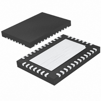
LTC2449CUHF Linear Technology, LTC2449CUHF Datasheet - Page 26

LTC2449CUHF
Manufacturer Part Number
LTC2449CUHF
Description
IC ADC 24BIT HI SPEED 38QFN
Manufacturer
Linear Technology
Datasheet
1.LTC2445CUHFPBF.pdf
(28 pages)
Specifications of LTC2449CUHF
Number Of Bits
24
Sampling Rate (per Second)
8k
Data Interface
MICROWIRE™, Serial, SPI™
Number Of Converters
1
Power Dissipation (max)
40mW
Voltage Supply Source
Single Supply
Operating Temperature
0°C ~ 70°C
Mounting Type
Surface Mount
Package / Case
38-WFQFN, Exposed Pad
Lead Free Status / RoHS Status
Contains lead / RoHS non-compliant
Available stocks
Company
Part Number
Manufacturer
Quantity
Price
Company:
Part Number:
LTC2449CUHF
Manufacturer:
LT
Quantity:
10 000
Part Number:
LTC2449CUHF
Manufacturer:
LINEAR/凌特
Quantity:
20 000
Part Number:
LTC2449CUHF#PBF
Manufacturer:
LINEAR/凌特
Quantity:
20 000
Part Number:
LTC2449CUHF#TRPBF
Manufacturer:
LINEAR/凌特
Quantity:
20 000
APPLICATIO S I FOR ATIO
LTC2444/LTC2445/
LTC2448/LTC2449
Example:
If an amplifier (e.g. LT1219) driving the input of an
LTC2444/LTC2445/LTC2448/LTC2449 has wideband
noise of 33nV/√Hz, band-limited to 1.8MHz, the total
noise entering the ADC input is:
When the ADC digitizes the input, its digital filter filters out
the wideband noise from the input signal. The noise
reduction depends on the oversample ratio which defines
the effective bandwidth of the digital filter.
At an oversample of 256, the noise bandwidth of the ADC
is 787Hz which reduces the total amplifier noise to:
The total noise is the RMS sum of this noise with the 2µV
noise of the ADC at OSR=256.
Increasing the oversample ratio to 32768 reduces the
noise bandwidth of the ADC to 6.2Hz which reduces the
total amplifier noise to:
The total noise is the RMS sum of this noise with the 200nV
noise of the ADC at OSR = 32768.
In this way, the digital filter with its variable oversampling
ratio can greatly reduce the effects of external noise
sources.
26
33nV/√Hz • √1.8MHz = 44.3µV.
33nV/√Hz • √787Hz = 0.93µV.
√
33nV/√Hz • √6.2Hz = 82nV.
√
(0.93µV)
(82nV)
2
+ (200nV)
2
+ (2uV)
U
2
2
ANALOG INPUT
= 2.2µV.
= 216nV.
U
–0.5V
0.1V TO V
1,4,5,6,31,32,33,39
REFERENCE
VOLTAGE
0.5V
REF
1µF
4.5V TO 5.5V
REF
TO
CC
W
28
29
30
8
9
V
REF
REF
CH0
CH1
GND
CC
•
•
•
LTC2448
Figure 16. Simple External Clock Source
+
–
BUSY
SDO
U
SCK
EXT
CS
F
O
2
35
38
37
36
3
3-WIRE
SPI INTERFACE
Automatic Offset Calibration of External
Buffers/Amplifiers
The LTC2445/LTC2449 enable an external amplifier to be
inserted between the multiplexer output and the ADC
input. This enables one external buffer/amplifier circuit to
be shared between all 17 analog inputs (16 single-ended
or 8 differential). The LTC2445/LTC2449 perform an inter-
nal offset calibration every conversion cycle in order to
remove the offset and drift of the ADC. This calibration is
performed through a combination of front end switching
and digital processing. Since the external amplifier is
placed between the multiplexer and the ADC, it is inside the
correction loop. This results in automatic offset correction
and offset drift removal of the external amplifier.
The LT1368 is an excellent amplifier for this function. It
has rail-to-rail inputs and outputs, and it operates on a
single 5V supply. Its open-loop gain is 1M and its input
bias current is 10nA. It also requires at least a 0.1µF load
capacitor for compensation. It is this feature that sets it
apart from other amplifiers—the load capacitor attenu-
ates sampling glitches from the LTC2445/LTC2449 ADCIN
terminals, allowing it to achieve full performance of the
ADC with high impedance at the multiplexer inputs.
Another benefit of the LT1368 is that it can be powered
from supplies equal to or greater than that of the ADC. This
can allow the inputs to span the entire absolute maximum
of GND – 0.3V to V
7.5V to 10V and a negative supply of –2.5 to –5V gives the
amplifier plenty of headroom over the LTC2445/LTC2449
input range.
NC
OUT
DIV
LTC1799
GND
SET
V
+
CC
+ 0.3V. Using a positive supply of
0.1µF
24448 F17
R
SET
2444589fb


