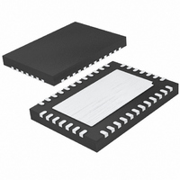
LTC2449CUHF Linear Technology, LTC2449CUHF Datasheet - Page 6

LTC2449CUHF
Manufacturer Part Number
LTC2449CUHF
Description
IC ADC 24BIT HI SPEED 38QFN
Manufacturer
Linear Technology
Datasheet
1.LTC2445CUHFPBF.pdf
(28 pages)
Specifications of LTC2449CUHF
Number Of Bits
24
Sampling Rate (per Second)
8k
Data Interface
MICROWIRE™, Serial, SPI™
Number Of Converters
1
Power Dissipation (max)
40mW
Voltage Supply Source
Single Supply
Operating Temperature
0°C ~ 70°C
Mounting Type
Surface Mount
Package / Case
38-WFQFN, Exposed Pad
Lead Free Status / RoHS Status
Contains lead / RoHS non-compliant
Available stocks
Company
Part Number
Manufacturer
Quantity
Price
Company:
Part Number:
LTC2449CUHF
Manufacturer:
LT
Quantity:
10 000
Part Number:
LTC2449CUHF
Manufacturer:
LINEAR/凌特
Quantity:
20 000
Part Number:
LTC2449CUHF#PBF
Manufacturer:
LINEAR/凌特
Quantity:
20 000
Part Number:
LTC2449CUHF#TRPBF
Manufacturer:
LINEAR/凌特
Quantity:
20 000
PI FU CTIO S
LTC2444/LTC2445/
LTC2448/LTC2449
GND – 0.3V to V
selected inputs (IN
(V
input range, the converter produces unique over-range
and under-range output codes.
CH0 to CH15 (Pins 8-23): LTC2448/LTC2449 Analog
Inputs. May be programmed for single-ended or differen-
tial mode.
CH0 to CH7 (Pins 9, 10, 13, 14, 17, 18, 21, 22): LTC2444/
LTC2445 Analog Inputs. May be programmed for single-
ended or differential mode.
NC (Pins 8, 11, 12, 15, 16, 19, 20, 23): LTC2444/
LTC2445 No Connect/Channel Isolation Shield. May be
left floating or tied to any voltage 0 to V
provide isolation for pairs of differential input channels.
NC (Pins 24, 25, 26, 27): LTC2444/LTC2448 No Connect.
These pins can either be tied to ground or left floating.
MUXOUTP (Pin 24): LTC2445/LTC2449 Positive Multi-
plexer Output. Used to drive the input to an external buffer/
amplifier.
ADCINP (Pin 25): LTC2445/LTC2449 Positive ADC Input.
Tie to output of buffer/amplifier driven by MUXOUTP.
ADCINN (Pin 26): LTC2445/LTC2449 Negative ADC Input.
Tie to output of buffer/amplifier driven by MUXOUTN.
MUXOUTN (Pin 27): LTC2445/LTC2449 Negative Multi-
plexer Output. Used to drive the input to an external buffer/
amplifier.
V
a 10µF tantalum capacitor in parallel with a 0.1µF ceramic
capacitor as close to the part as possible.
REF
Input. The voltage on these pins can have any value
between GND and V
input, REF
reference input, REF
SDI (Pin 34): Serial Data Input. This pin is used to select
the speed, 1X or 2X mode, resolution, and input channel,
for the next conversion cycle. At initial power up, the
default mode of operation is CH0-CH1, OSR of 256, and 1X
mode. The serial data input contains an enable bit which
6
CC
IN
U
(Pin 28): Positive Supply Voltage. Bypass to GND with
= IN
+
(Pin 29), REF
+
– IN
+
U
, is maintained more positive than the negative
–
) from –0.5 • V
CC
+
and IN
+ 0.3V. Within these limits, the two
+
CC
U
, by at least 0.1V.
–
as long as the reference positive
(Pin 30): Differential Reference
–
) provide a bipolar input range
REF
to 0.5 • V
REF
CC
. Outside this
in order to
determines if a new channel/speed is selected. If this bit is
low the following conversion remains at the same speed
and selected channel. The serial data input is applied to the
device under control of the serial clock (SCK) during the
data output cycle. The first conversion following a new
channel/speed is valid.
F
controls the internal conversion clock. When F
nected to V
oscillator running at 9MHz. The conversion rate is deter-
mined by the selected OSR such that t
OSR + 170/f
at 8/t
60Hz) at OSR = 32768. This pin may be driven with a
maximum external clock of 10.24MHz resulting in a maxi-
mum 8kHz output rate (OSR = 64, 2X Mode).
CS (Pin 36): Active Low Chip Select. A LOW on this pin
enables the SDO ditital output and wakes up the ADC.
Following each conversion the ADC automatically enters
the sleep mode and remains in this low power state as long
as CS is HIGH. A LOW-to-HIGH transition on CS during the
Data Output aborts the data transfer and starts a new
conversion.
SDO (Pin 37): Three-State Digital Output. During the data
output period, this pin is used as serial data output. When
the chip select CS is HIGH (CS = V
high impedance state. During the conversion and sleep
periods, this pin is used as the conversion status output.
The conversion status can be observed by pulling CS
LOW. This signal is HIGH while the conversion is in
progress and goes LOW once the conversion is complete.
SCK (Pin 38): Bidirectional Digital Clock Pin. In internal
serial clock operation mode, SCK is used as a digital output
for the internal serial interface clock during the data output
period. In the external serial clock operation mode, SCK is
used as the digital input for the external serial interface
clock during the data output period. The serial clock
operation mode is determined by the logic level applied to
the EXT pin.
Exposed Pad (Pin 39): Ground. The exposed pad on the
bottom of the package must be soldered to the PCB ground.
For prototyping purposes, this pin may remain floating.
O
(Pin 35): Frequency Control Pin. Digital input that
CONV
, 7kHz at OSR = 256 and 55Hz (Simultaneous 50/
OSC
CC
or GND, the converter uses its internal
(kHz). The first digital filter null is located
CC
) the SDO pin is in a
CONV
(ms) = 40 •
O
is con-
2444589fb


