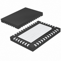
LTC2449CUHF#TR Linear Technology, LTC2449CUHF#TR Datasheet - Page 23

LTC2449CUHF#TR
Manufacturer Part Number
LTC2449CUHF#TR
Description
IC ADC 24BIT HI SPEED 38QFN
Manufacturer
Linear Technology
Datasheet
1.LTC2445CUHFPBF.pdf
(28 pages)
Specifications of LTC2449CUHF#TR
Number Of Bits
24
Sampling Rate (per Second)
8k
Data Interface
MICROWIRE™, Serial, SPI™
Number Of Converters
1
Power Dissipation (max)
40mW
Voltage Supply Source
Single Supply
Operating Temperature
0°C ~ 70°C
Mounting Type
Surface Mount
Package / Case
38-WFQFN, Exposed Pad
Lead Free Status / RoHS Status
Contains lead / RoHS non-compliant
Available stocks
Company
Part Number
Manufacturer
Quantity
Price
APPLICATIO S I FOR ATIO
If F
1.8MHz ±5% (over supply and temperature variations). At
an OSR of 32,768, the first NULL is at f
latency output rate is f
the noise performance of the device is 280nV
LTC2448) and 200nV
than 80dB rejection of 50Hz ±2% and 60Hz ±2%. Since the
OSR is large (32,768) the wide band rejection is extremely
large and the antialiasing requirements are simple. The
first multiple of f
Figure 12.
The first NULL becomes f
(an output rate of 880Hz) and F
NULL has shifted, the sample rate remains constant. As a
result of constant modulator sampling rate, the linearity,
offset and full-scale performance remains unchanged as
does the first multiple of f
The sample rate f
driving the F
rate is f
O
is grounded, f
Figure 12. LTC2444/LTC2445/LTC2448/LTC2449
Normal Mode Rejection (Internal Oscillator)
S
= f
–100
–120
–140
–20
–60
–40
–80
O
EOSC
0
pin with an external oscillator. The sample
0
DIFFERENTIAL INPUT SIGNAL FREQUENCY (Hz)
S
/5, where f
S
occurs at 55Hz • 32,768 = 1.8MHz, see
and NULL f
U
S
RMS
N
is set by the on-chip oscillator at
/8 = 6.9Hz. At the maximum OSR,
REJECTION > 120dB
(LTC2445/LTC2449) with better
N
U
S
= 7.04kHz with an OSR of 256
.
1000000
EOSC
N
, may also be adjusted by
O
is the frequency of the
W
grounded. While the
1.8MHz
N
= 55Hz and the no
1440 F13
RMS
2000000
U
(LTC2444/
clock applied to F
sample rate leads to notch frequencies f
maintaining simple antialiasing requirements. A 100kHz
clock applied to F
harmonics up to 20kHz, see Figure 13. This is useful in
applications requiring digitalization of the DC component
of a noisy input signal and eliminates the need of placing
a 0.6Hz filter in front of the ADC.
An external oscillator operating from 100kHz to 20MHz
can be implemented using the LTC1799 (resistor set
SOT-23 oscillator), see Figure 16. By floating pin 4 (DIV)
of the LTC1799, the output oscillator frequency is:
The normal mode rejection characteristic shown in
Figure 13 is achieved by applying the output of the LTC1799
(with R
LTC2448/LTC2449 with SDI tied HIGH (OSR = 32768).
Figure 13. LTC2444/LTC2445/LTC2448/LTC2449 Normal
Mode Rejection (External Oscillator at 90kHz)
SET
f
OSC
= 100k) to the F
–120
–140
–100
–20
–40
–60
–80
0
=
0
DIFFERENTIAL INPUT SIGNAL FREQUENCY (Hz)
10
O
LTC2444/LTC2445/
. Combining a large OSR with a reduced
MHz
O
LTC2448/LTC2449
2
results in a NULL at 0.6Hz plus all
•
⎛
⎜
⎝
O
10
4
pin on the LTC2444/LTC2445/
10
•
R
k
SET
6
⎞
⎟
⎠
8
N
2440 F14
near DC while
10
23
2444589fb


