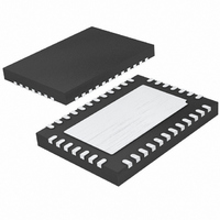
LTC2449CUHF#TR Linear Technology, LTC2449CUHF#TR Datasheet - Page 7

LTC2449CUHF#TR
Manufacturer Part Number
LTC2449CUHF#TR
Description
IC ADC 24BIT HI SPEED 38QFN
Manufacturer
Linear Technology
Datasheet
1.LTC2445CUHFPBF.pdf
(28 pages)
Specifications of LTC2449CUHF#TR
Number Of Bits
24
Sampling Rate (per Second)
8k
Data Interface
MICROWIRE™, Serial, SPI™
Number Of Converters
1
Power Dissipation (max)
40mW
Voltage Supply Source
Single Supply
Operating Temperature
0°C ~ 70°C
Mounting Type
Surface Mount
Package / Case
38-WFQFN, Exposed Pad
Lead Free Status / RoHS Status
Contains lead / RoHS non-compliant
Available stocks
Company
Part Number
Manufacturer
Quantity
Price
APPLICATIO S I FOR ATIO
CONVERTER OPERATION
Converter Operation Cycle
The LTC2444/LTC2445/LTC2448/LTC2449 are multi-
channel, high speed, delta-sigma analog-to-digital con-
verters with an easy to use 3- or 4-wire serial interface (see
Figure 1). Their operation is made up of three states. The
converter operating cycle begins with the conversion,
followed by the low power sleep state and ends with the
data output/input (see Figure 2). The 4-wire interface
consists of serial data input (SDI), serial data output
(SDO), serial clock (SCK) and chip select (CS). The inter-
face, timing, operation cycle and data out format is com-
patible with Linear’s entire family of ∆Σ converters.
FU CTIO AL BLOCK DIAGRA
TEST CIRCUITS
U
GND
U
V
SDO
CC
U
CH15
REF
REF
Hi-Z TO V
V
V
COM
1.69k
CH0
CH1
OL
OH
+
–
TO V
TO Hi-Z
U
OH
OH
•
•
•
C
MUX
LOAD
W
2440 TA03
= 20pF
IN
IN
+
–
Figure 1. Functional Block Diagram
∆Σ MODULATOR
–
DIFFERENTIAL
U
3RD ORDER
W
+
AUTOCALIBRATION
DECIMATING FIR
AND CONTROL
ADDRESS
Figure 2. LTC2444/LTC2445/LTC2448/LTC2449
State Transition Diagram
LTC2444/LTC2445/
LTC2448/LTC2449
SDO
OSCILLATOR
INTERFACE
INTERNAL
SERIAL
Hi-Z TO V
V
V
OH
OL
OSR=256,1X MODE
IN
CHANNEL SELECT
SPEED SELECT
2444 F01
V
DATA OUTPUT
TO Hi-Z
+
TO V
CC
=CH0, IN
POWER UP
CONVERT
CS = LOW
SCK
1.69k
SLEEP
AND
OL
C
OL
LOAD
–
=CH1
2444 F02
2440 TA04
= 20pF
F
(INT/EXT)
SDI
SCK
SDO
CS
O
2444589fb
7


