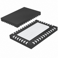
LTC2449CUHF#TR Linear Technology, LTC2449CUHF#TR Datasheet - Page 9

LTC2449CUHF#TR
Manufacturer Part Number
LTC2449CUHF#TR
Description
IC ADC 24BIT HI SPEED 38QFN
Manufacturer
Linear Technology
Datasheet
1.LTC2445CUHFPBF.pdf
(28 pages)
Specifications of LTC2449CUHF#TR
Number Of Bits
24
Sampling Rate (per Second)
8k
Data Interface
MICROWIRE™, Serial, SPI™
Number Of Converters
1
Power Dissipation (max)
40mW
Voltage Supply Source
Single Supply
Operating Temperature
0°C ~ 70°C
Mounting Type
Surface Mount
Package / Case
38-WFQFN, Exposed Pad
Lead Free Status / RoHS Status
Contains lead / RoHS non-compliant
Available stocks
Company
Part Number
Manufacturer
Quantity
Price
APPLICATIO S I FOR ATIO
LTC2448/LTC2449 convert the bipolar differential input
signal, V
input channels), from – FS = – 0.5 • V
where V
verter indicates the overrange or the underrange condition
using distinct output codes.
MUXOUT/ADCIN
There are two differences between the LTC2444/LTC2448
and the LTC2445/LTC2449. The first is the RMS noise
performance. For a given OSR, the LTC2445/LTC2449
noise level is approximately √2 times lower (0.5 effective
bits)than that of the LTC2444/LTC2448.
The second difference is the LTC2445/LTC2449 includes
MUXOUT/ADCIN pins. These pins enable an external buffer
or gain block to be inserted between the output of the
multiplexer and the input to the ADC. Since the buffer is
driven by the output of the multiplexer, only one circuit is
required for all 16 input channels. Additionally, the trans-
parent calibration feature of the LTC244X family automati-
cally removes the offset errors of the external buffer.
In order to achieve optimum performance, the MUXOUT
and ADCIN pins should not be shorted together. In appli-
cations where the MUXOUT and ADCIN need to be shorted
together, the LTC2444/LTC2448 should be used because
the MUXOUT and ADCIN are internally connected for
optimum performance.
Output Data Format
The LTC2444/LTC2445/LTC2448/LTC2449 serial output
data stream is 32 bits long. The first 3 bits represent status
information indicating the sign and conversion state. The
next 24 bits are the conversion result, MSB first. The
remaining 5 bits are sub LSBs beyond the 24-bit level that
may be included in averaging or discarded without loss of
resolution. In the case of ultrahigh resolution modes,
more than 24 effective bits of performance are possible
(see Table 5). Under these conditions, sub LSBs are
included in the conversion result and represent useful
information beyond the 24-bit level. The third and fourth
bit together are also used to indicate an underrange
condition (the differential input voltage is below –FS) or an
overrange condition (the differential input voltage is above
+FS).
REF
IN
= IN
= REF
+
– IN
+
U
– REF
–
(where IN
U
–
. Outside this range, the con-
+
and IN
W
REF
to +FS = 0.5 • V
–
are the selected
U
REF
Bit 31 (first output bit) is the end of conversion (EOC)
indicator. This bit is available at the SDO pin during the
conversion and sleep states whenever the CS pin is LOW.
This bit is HIGH during the conversion and goes LOW
when the conversion is complete.
Bit 30 (second output bit) is a dummy bit (DMY) and is
always LOW.
Bit 29 (third output bit) is the conversion result sign indi-
cator (SIG). If V
bit is LOW.
Bit 28 (fourth output bit) is the most significant bit (MSB)
of the result. This bit in conjunction with Bit 29 also
provides the underrange or overrange indication. If both
Bit 29 and Bit 28 are HIGH, the differential input voltage is
above +FS. If both Bit 29 and Bit 28 are LOW, the
differential input voltage is below –FS.
The function of these bits is summarized in Table 1.
Table 1. LTC2444/LTC2445/LTC2448/LTC2449 Status Bits
Input Range
V
0V ≤ V
–0.5 • V
V
Bits 28-5 are the 24-bit conversion result MSB first.
Bit 5 is the least significant bit (LSB).
Bits 4-0 are sub LSBs below the 24-bit level. Bits 4-0 may
be included in averaging or discarded without loss of
resolution.
Data is shifted out of the SDO pin under control of the serial
clock (SCK), see Figure 3. Whenever CS is HIGH, SDO
remains high impedance and SCK is ignored.
In order to shift the conversion result out of the device, CS
must first be driven LOW. EOC is seen at the SDO pin of the
device once CS is pulled LOW. EOC changes real time from
HIGH to LOW at the completion of a conversion. This
signal may be used as an interrupt for an external
microcontroller. Bit 31 (EOC) can be captured on the first
rising edge of SCK. Bit 30 is shifted out of the device on the
IN
IN
≥ 0.5 • V
< – 0.5 • V
IN
REF
< 0.5 • V
≤ V
REF
REF
IN
REF
< 0V
IN
is >0, this bit is HIGH. If V
LTC2444/LTC2445/
LTC2448/LTC2449
Bit 31 Bit 30 Bit 29 Bit 28
EOC
0
0
0
0
DMY
0
0
0
0
IN
SIG
is <0, this
1
1
0
0
2444589fb
MSB
9
1
0
1
0


