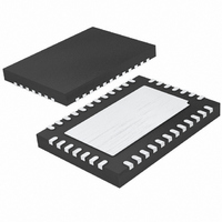
LTC2449CUHF#TRPBF Linear Technology, LTC2449CUHF#TRPBF Datasheet - Page 20

LTC2449CUHF#TRPBF
Manufacturer Part Number
LTC2449CUHF#TRPBF
Description
IC ADC 24BIT HI SPEED 38QFN
Manufacturer
Linear Technology
Datasheet
1.LTC2445CUHFPBF.pdf
(28 pages)
Specifications of LTC2449CUHF#TRPBF
Number Of Bits
24
Sampling Rate (per Second)
8k
Data Interface
MICROWIRE™, Serial, SPI™
Number Of Converters
1
Power Dissipation (max)
40mW
Voltage Supply Source
Single Supply
Operating Temperature
0°C ~ 70°C
Mounting Type
Surface Mount
Package / Case
38-WFQFN, Exposed Pad
Lead Free Status / RoHS Status
Lead free / RoHS Compliant
Available stocks
Company
Part Number
Manufacturer
Quantity
Price
APPLICATIO S I FOR ATIO
LTC2444/LTC2445/
LTC2448/LTC2449
If CS remains LOW longer than t
edge of SCK will occur and the conversion result is serially
shifted out of the SDO pin. The data output cycle begins on
this first rising edge of SCK and concludes after the 32nd
rising edge. Data is shifted out the SDO pin on each falling
edge of SCK. The internally generated serial clock is output
to the SCK pin. This signal may be used to shift the
conversion result into external circuitry. EOC can be
latched on the first rising edge of SCK and the last bit of the
conversion result on the 32nd rising edge of SCK. After the
32nd rising edge, SDO goes HIGH (EOC = 1), SCK stays
HIGH and a new conversion starts.
Typically, CS remains LOW during the data output state.
However, the data output state may be aborted by pulling
CS HIGH anytime between the first and 32nd rising edge
20
CONVERSION
BUSY
SDO
SCK
SDI
CS
SLEEP
U
DATA OUTPUT
DON'T CARE
<t
1
EOC(TEST)
U
5
Figure 8. Internal Serial Clock, Reduced Data Output Length
EOCtest
CONVERSION
W
0.1V TO V
REFERENCE
ANALOG
Hi-Z
INPUTS
VOLTAGE
, the first rising
1µF
4.5V TO 5.5V
CC
BIT 31
EOC
1
•
•
•
•
•
•
U
28
29
30
15
16
23
8
7
BIT 30
V
REF
REF
CH0
CH7
CH8
CH15
COM
“0”
2
CC
•
•
•
•
•
•
LTC2448
+
–
BIT 29
SIG
BUSY
3
DON'T CARE
GND
SDO
SCK
SDI
DATA OUTPUT
CS
F
O
BIT 28 BIT 27 BIT 26 BIT 25
MSB
of SCK, see Figure 8. On the rising edge of CS, the device
aborts the data output state and immediately initiates a
new conversion. This is useful for systems not requiring
all 32 bits of output data, aborting an invalid conversion
cycle, or synchronizing the start of a conversion. Thirteen
serial input data bits are required in order to properly
program the speed/resolution and input channel. If the
data output sequence is aborted prior to the 13th rising
edge of SCK, the new input data is ignored, and the
previously selected speed/resolution and channel are used
for the next conversion cycle. If a new channel is being
programmed, the rising edge of CS must come after the
14th falling edge of SCK in order to store the data input
sequence.
37
2
1,4,5,6,31,32,33,39
4
38
34
35
36
5
4-WIRE
SPI INTERFACE
= EXTERNAL OSCILLATOR
= INTERNAL OSCILLATOR
6
Hi-Z
CONVERSION
TEST EOC
DON'T CARE
SLEEP
2444 F09
<t
EOC(TEST)
2444589fb


