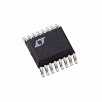
LTC1867CGN Linear Technology, LTC1867CGN Datasheet

LTC1867CGN
Specifications of LTC1867CGN
Available stocks
Related parts for LTC1867CGN
LTC1867CGN Summary of contents
Page 1
... The signal-to-noise ratio (SNR) for the LTC1867 is typically 89dB, with the internal reference. Housed in a compact, narrow 16-pin SSOP package, the LTC1863/LTC1867 can be used in space-sensitive as well as low-power applications. L, LT, LTC and LTM are registered trademarks of Linear Technology Corporation. All other trademarks are the property of their respective owners ...
Page 2
... ORDER INFORMATION LEAD FREE FINISH TAPE AND REEL LTC1863CGN#PBF LTC1863CGN#TRPBF LTC1863IGN#PBF LTC1863IGN#TRPBF LTC1867CGN#PBF LTC1867CGN#TRPBF LTC1867IGN#PBF LTC1867IN#TRPBF LTC1867ACGN#PBF LTC1867ACGN#TRPBF LTC1867AIGN #PBF LTC1867AIGN#TRPBF Consult LTC Marketing for parts specifi ed with wider operating temperature ranges. *The temperature grade is identifi label on the shipping container. ...
Page 3
CONVERTER CHARACTERISTICS temperature range, otherwise specifi cations are at T PARAMETER CONDITIONS Gain Error Match Gain Error Tempco Internal Reference External Reference Power Supply Sensitivity V = 4.75V – 5.25V DD DYNAMIC ACCURACY SYMBOL PARAMETER SNR Signal-to-Noise Ratio S/(N+D) Signal-to-(Noise ...
Page 4
LTC1863/LTC1867 DIGITAL INPUTS AND DIGITAL OUTPUTS full operating temperature range, otherwise specifi cations are at T SYMBOL PARAMETER C Digital Input Capacitance IN V High Level Output Voltage (SDO Low Level Output Voltage (SDO Output Source ...
Page 5
TIMING CHARACTERISTICS range, otherwise specifi cations are Note 4: When these pin voltages are taken below GND, they will be clamped by internal diodes. This product can handle input currents of greater than 100mA below GND without ...
Page 6
LTC1863/LTC1867 TYPICAL PERFORMANCE CHARACTERISTICS (LTC1867) Signal-to-Noise Ratio vs Frequency 100 INPUT FREQUENCY (kHz) 18637 G07 (LTC1863/LTC1867) Supply Current vs f SAMPLE 2 1.5 1.0 0.5 0 ...
Page 7
PIN FUNCTIONS CHO-CH7/COM (Pins 1-8): Analog Input Pins. Analog inputs must be free of noise with respect to GND. CH7/COM can be either a separate channel or the common minus input for the other channels. REFCOMP (Pin 9): Reference Buffer ...
Page 8
LTC1863/LTC1867 TIMING DIAGRAMS (For Short Pulse Mode CS/CONV 50% t (SDO Valid After CONV↓ CS/CONV 0.4V Hi-Z SDO t (SLEEP Mode Wake-Up Time SCK 50% SLEEP BIT (SLP = 0) ...
Page 9
APPLICATIONS INFORMATION Analog Input Multiplexer The analog input multiplexer is controlled by a 7-bit input data word. The input data word is defi ned as follows COM UNI SLP SD = SINGLE/DIFFERENTIAL BIT OS = ODD/SIGN ...
Page 10
... The following list is a summary of the op amps that are suitable for driving the LTC1863/LTC1867. More detailed information is available in the Linear Technology data books or Linear Technology website. LT1007 - Low noise precision amplifi er. 2.7mA supply current ± ±15V supplies. Gain bandwidth product 8MHz. DC applications. LT1097 - Low cost, low power precision amplifi ...
Page 11
APPLICATIONS INFORMATION 50Ω ANALOG CH0 INPUT 2000pF GND REFCOMP 10μF Figure 1a. Optional RC Input Filtering for Single-Ended Input 1000pF 50Ω DIFFERENTIAL ANALOG 1000pF 50Ω INPUTS 1000pF 10μF Figure 1b. Optional RC Input Filtering for Differential Inputs DC Performance One ...
Page 12
LTC1863/LTC1867 APPLICATIONS INFORMATION where V is the RMS amplitude of the fundamental 1 frequency and V through V are the amplitudes of the 2 N second through Nth harmonics. Internal Reference The LTC1863/LTC1867 has an on-chip, temperature compensated, curvature corrected, ...
Page 13
APPLICATIONS INFORMATION If the CS/CONV returns low during a bit decision, it can create a small error. For best performance ensure that the CS/CONV returns low either within 100ns after the conver- sion starts (i.e. before the fi rst bit ...
Page 14
LTC1863/LTC1867 APPLICATIONS INFORMATION CS/CONV SCK 1 2 SDI SD 0S DON'T CARE t CONV SDO MSB = D11 D10 (LTC1863) Hi-Z t CONV SDO MSB = D15 D14 D13 (LTC1867) Hi-Z Figure 7. Example 2, CS/CONV Starts a Conversion With ...
Page 15
... FLASH SHALL NOT EXCEED 0.010" (0.254mm) PER SIDE Information furnished by Linear Technology Corporation is believed to be accurate and reliable. However, no responsibility is assumed for its use. Linear Technology Corporation makes no representa- tion that the interconnection of its circuits as described herein will not infringe on existing patent rights. ...
Page 16
... SO-8 and MSOP Packages 450μA at 150ksps, 10μA at 1ksps, SO-8 and MSOP Packages 850μA at 250ksps, 2μA at 1ksps, SO-8 and MSOP Packages 450μA at 150ksps, 10μA at 1ksps, SO-8 and MSOP Packages www.linear.com ● 18637fa LT 0209 REV A • PRINTED IN USA © LINEAR TECHNOLOGY CORPORATION 2008 ...


