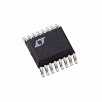
LTC1867LCGN#TRPBF Linear Technology, LTC1867LCGN#TRPBF Datasheet

LTC1867LCGN#TRPBF
Specifications of LTC1867LCGN#TRPBF
Available stocks
Related parts for LTC1867LCGN#TRPBF
LTC1867LCGN#TRPBF Summary of contents
Page 1
... INL specifi cation and 16-bit no missing codes over temperature. Housed in a compact, narrow 16-pin SSOP package, the LTC1863L/LTC1867L can be used in space-sensitive as well as low power applications. , LT, LTC and LTM are registered trademarks of Linear Technology Corporation. All other trademarks are the property of their respective owners. LTC1863L/LTC1867L 16 V ...
Page 2
... ORDER INFORMATION LEAD FREE FINISH TAPE AND REEL LTC1863LCGN#PBF LTC1863LCGN#TRPBF LTC1863LIGN#PBF LTC1863LIGN#TRPBF LTC1867LCGN#PBF LTC1867LCGN#TRPBF LTC1867LIGN#PBF LTC1867LIGN#TRPBF LTC1867LACGN#PBF LTC1867LACGN#TRPBF LTC1867LAIGN#PBF LTC1867LAIGN#TRPBF Consult LTC Marketing for parts specifi ed with wider operating temperature ranges. *The temperature grade is identifi label on the shipping container. ...
Page 3
CONVERTER CHARACTERISTICS temperature range, otherwise specifi cations are at T PARAMETER CONDITIONS Gain Error Unipolar Bipolar Gain Error Match Unipolar Bipolar Gain Error Tempco Internal Reference External Reference Power Supply Sensitivity V = 2.7V – 3.6V DD DYNAMIC ACCURACY SYMBOL ...
Page 4
LTC1863L/LTC1867L DIGITAL INPUTS AND DIGITAL OUTPUTS full operating temperature range, otherwise specifi cations are at T SYMBOL PARAMETER I Digital Input Current IN C Digital Input Capacitance IN V High Level Output Voltage (SDO Low Level Output Voltage ...
Page 5
TIMING CHARACTERISTICS range, otherwise specifi cations are Note 4: When these pin voltages are taken below GND, they will be clamped by internal diodes. This product can handle input currents of greater than 100mA below GND without ...
Page 6
LTC1863L/LTC1867L TYPICAL PERFORMANCE CHARACTERISTICS (LTC1867L) Total Harmonic Distortion vs Input Frequency –100 –90 –80 SFDR –70 THD –60 –50 – –30 INTERNAL REF f = 175ksps SAMPLE – INPUT FREQUENCY (kHz) 1863L7L G07 (LTC1863L/ ...
Page 7
TYPICAL PERFORMANCE CHARACTERISTICS (LTC1863L/ LTC1867L) Integral Nonlinearity vs Output Code (LTC1863L) 1.00 0.75 0.50 0.25 0 –0.25 –0.50 –0.75 –1.00 0 512 1024 1536 2048 CODE PIN FUNCTIONS CHO-CH7/COM (Pins 1-8): Analog Input Pins. Analog inputs must be free of ...
Page 8
LTC1863L/LTC1867L TYPICAL CONNECTION DIAGRAM TEST CIRCUITS Load Circuits for Access Timing SDO SDO (A) Hi AND (B) Hi AND TIMING DIAGRAMS ...
Page 9
APPLICATIONS INFORMATION Overview The LTC1863L/LTC1867L are complete, low power, multi- plexed ADCs. They consist of a 12-/16-bit, 175ksps capaci- tive successive approximation A/D converter, a precision internal reference, a confi gurable 8-channel analog input multiplexer (MUX) and a serial port ...
Page 10
... LTC1863L/LTC1867L inputs can be driven directly. More acquisition time should be allowed for a higher impedance source. The following list is a summary of the op amps that are suitable for driving the LTC1863L/LTC1867L. More detailed information is available in the Linear Technology data books or Linear Technology website. 50Ω ANALOG CH0 ...
Page 11
APPLICATIONS INFORMATION many applications. For instance, Figure 1 shows a 50Ω source resistor and a 2000pF capacitor to ground on the input will limit the input bandwidth to 1.6MHz. The source impedance has to be kept low to avoid gain ...
Page 12
LTC1863L/LTC1867L APPLICATIONS INFORMATION Total Harmonic Distortion Total Harmonic Distortion (THD) is the ratio of the RMS sum of all harmonics of the input signal to the fundamental itself. The out-of-band harmonics alias into the frequency band between DC and half ...
Page 13
APPLICATIONS INFORMATION If the CS/CONV returns low during a bit decision, it can create a small error. For best performance ensure that the CS/CONV returns low either within 100ns after the conver- sion starts (i.e. before the fi rst bit ...
Page 14
LTC1863L/LTC1867L APPLICATIONS INFORMATION CS/CONV SCK 1 2 SDI DON'T CARE CONV SDO MSB = D11 D10 (LTC1863) Hi-Z t CONV SDO MSB = D15 D14 D13 (LTC1867) Hi-Z Figure 7. Example 2, CS/CONV Starts a Conversion With ...
Page 15
... FLASH SHALL NOT EXCEED 0.010" (0.254mm) PER SIDE Information furnished by Linear Technology Corporation is believed to be accurate and reliable. However, no responsibility is assumed for its use. Linear Technology Corporation makes no representa- tion that the interconnection of its circuits as described herein will not infringe on existing patent rights. ...
Page 16
... SO-8 and MSOP Packages 5V Supply, Pin Compatible with LTC1863L/LTC1867L 850μA at 250ksps, 2μA at 1ksps, SO-8 and MSOP Packages 450μA at 150ksps, 10μA at 1ksps, SO-8 and MSOP Packages www.linear.com ● 1863l7lfc LT 0209 REV C • PRINTED IN USA © LINEAR TECHNOLOGY CORPORATION 2005 ...


