LTC2224CUK#TR Linear Technology, LTC2224CUK#TR Datasheet
LTC2224CUK#TR
Specifications of LTC2224CUK#TR
Available stocks


Related parts for LTC2224CUK#TR


LTC2224CUK#TR Summary of contents
Page 1
... PECL, LVDS, TTL, or CMOS inputs. An optional clock duty cycle stabilizer allows high performance at full speed for a wide range of clock duty cycles. , LTC and LT are registered trademarks of Linear Technology Corporation. All other trademarks are the property of their respective owners. 3. ...
Page 2
LTC2224 ABSOLUTE AXI U RATI (Notes Supply Voltage (V ) ................................................. 4V DD Digital Output Ground Voltage (OGND) ....... –0. Analog Input Voltage (Note 3) ..... –0.3V ...
Page 3
ALOG I PUT The ● denotes the specifications which apply over the full operating temperature range, otherwise specifications are 25°C. (Note 4) A SYMBOL PARAMETER V Analog Input Range ( Analog ...
Page 4
LTC2224 TER AL REFERE CE CHARACTERISTICS PARAMETER V Output Voltage CM V Output Tempco CM V Line Regulation CM V Output Resistance DIGITAL I PUTS A D DIGITAL OUTPUTS full operating temperature range, ...
Page 5
W U POWER REQUIRE E TS range, otherwise specifications are at T SYMBOL PARAMETER V Analog Supply Voltage DD OV Output Supply Voltage DD I Analog Supply Current VDD P Power Dissipation DISS P Shutdown Power SHDN P Nap Mode ...
Page 6
LTC2224 W U TYPICAL PERFOR A CE CHARACTERISTICS LTC2224: INL, 2V Range 1.0 0.8 0.6 0.4 0.2 0 –0.2 –0.4 –0.6 –0.8 –1.0 0 1024 2048 3072 4096 OUTPUT CODE 2224 G01 LTC2224: SNR vs Input Frequency, –1dB, 2V Range ...
Page 7
W U TYPICAL PERFOR A CE CHARACTERISTICS LTC2224: SFDR and SNR vs Sample Rate, 2V Range 30MHz, –1dB IN 100 95 90 SFDR SNR 100 120 140 ...
Page 8
LTC2224 W U TYPICAL PERFOR A CE CHARACTERISTICS LTC2224: 8192 Point FFT 30MHz, –1dB, 2V Range IN 0 – 10 – 20 – 30 – 40 – 50 – 60 – 70 – 80 – 90 – 100 ...
Page 9
CTIO (Pin 1): Positive Differential Analog Input – (Pin 2): Negative Differential Analog Input. IN REFHA (Pins 3, 4): ADC High Reference. Bypass to Pins 5, 6 with 0.1µF ceramic ...
Page 10
LTC2224 U U FUNCTIONAL BLOCK DIAGRA + A IN INPUT FIRST PIPELINED S/H ADC STAGE – 1.6V CM REFERENCE 2.2µF RANGE SELECT REF SENSE BUF 10 W SECOND PIPELINED THIRD PIPELINED ADC STAGE ADC STAGE REFH REFL ...
Page 11
DIAGRA S ANALOG N INPUT – ENC + ENC D0-D11, OF CLOCKOUT OE DATA Timing Diagram – ...
Page 12
LTC2224 U U APPLICATIO S I FOR ATIO DYNAMIC PERFORMANCE Signal-to-Noise Plus Distortion Ratio The signal-to-noise plus distortion ratio [S/(N + D)] is the ratio between the RMS amplitude of the fundamental input frequency and the RMS amplitude of all ...
Page 13
U U APPLICATIO S I FOR ATIO CONVERTER OPERATION As shown in Figure 1, the LTC2224 is a CMOS pipelined multistep converter. The converter has five pipelined ADC stages; a sampled analog input will result in a digitized value five ...
Page 14
LTC2224 U U APPLICATIO S I FOR ATIO During the sample phase when ENC is low, the transistors connect the analog inputs to the sampling capacitors and they charge to, and track the differential input voltage. When ENC transitions from ...
Page 15
U U APPLICATIO S I FOR ATIO signal at its optimum DC level. Terminating on the trans- former secondary is desirable, as this provides a common mode path for charging glitches caused by the sample and hold. Figure 3 shows ...
Page 16
LTC2224 U U APPLICATIO S I FOR ATIO 0.1µF 12Ω ANALOG INPUT 0.1µF 25Ω T1 0.1µF 25Ω 12Ω MA/COM ETC1-1-13 RESISTORS, CAPACITORS ARE 0402 PACKAGE SIZE Figure 6. Recommended Front End Circuit for Input Frequencies Between 100MHz and ...
Page 17
U U APPLICATIO S I FOR ATIO Input Range The input range can be set based on the application. The 2V input range will provide the best signal-to-noise perfor- mance while maintaining excellent SFDR. The 1V input range will have ...
Page 18
LTC2224 U U APPLICATIO S I FOR ATIO DIGITAL OUTPUTS Table 1 shows the relationship between the analog input voltage, the digital data bits and the overflow bit. Table 1. Output Codes vs Input Voltage + – A – A ...
Page 19
U U APPLICATIO S I FOR ATIO Overflow Bit The converter is either overranged or underranged when OF outputs a logic high. Output Clock The ADC has a delayed version of the ENC as a digital output, CLOCKOUT. The CLOCKOUT ...
Page 20
LTC2224 U U APPLICATIO S I FOR ATIO Clock Sources for Undersampling Undersampling raises the bar on the clock source and the higher the input frequency, the greater the sensitivity to clock jitter or phase noise. A clock source that ...
Page 21
U U APPLICATIO S I FOR ATIO R19 R1* C1 OPT 0.1µF T1* R2 ANALOG 24.9Ω INPUT J1 C2* R4 24.9Ω C3 0.1µF R6 50Ω 0.1µ 1µF 0.1µF ...
Page 22
LTC2224 U U APPLICATIO S I FOR ATIO Layer 1 Component Side Layer 3 Power Plane Silkscreen Top Layer 2 GND Plane Layer 4 Bottom Side 2224fa ...
Page 23
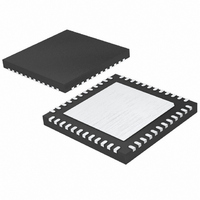
... PIN 1 TOP MARK (SEE NOTE 6) Information furnished by Linear Technology Corporation is believed to be accurate and reliable. However, no responsibility is assumed for its use. Linear Technology Corporation makes no represen- tation that the interconnection of its circuits as described herein will not infringe on existing patent rights Package 48-Lead Plastic QFN (7mm × ...
Page 24
... High IIP3: 20dBm at 1.9GHz, Integrated LO Quadrature Generator High IIP3: 21.5dBm at 900MHz, Integrated LO Quadrature Generator High IIP3: 21dBm at 800MHz, Integrated LO Quadrature Generator 4.5V to 5.25V Supply, 25dBm IIP3 at 900MHz 12.5dB, 500Ω Single-Ended RF and LO Ports www.linear.com ● 2224fa LT 0106 REV A • PRINTED IN USA © LINEAR TECHNOLOGY CORPORATION 2004 ...