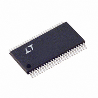
LTC1750IFW Linear Technology, LTC1750IFW Datasheet

LTC1750IFW
Specifications of LTC1750IFW
Available stocks
Related parts for LTC1750IFW
LTC1750IFW Summary of contents
Page 1
... DSPs or FIFOs. The 48-pin TSSOP package with a flow-through pinout simplifies the board layout. , LTC and LT are registered trademarks of Linear Technology Corporation. CORRECTION LOGIC AND S/H 14-BIT ...
Page 2
... External Reference (V = 1.125V) SENSE V = 1.125V, PGA = 0 SENSE CONDITIONS 4.75V V 5.25V DD + – 0 < < Sample Mode ENC < ENC Hold Mode ENC > ENC – + 1.5V < < INFORMATION ORDER PART TOP VIEW NUMBER OGND LTC1750CFW 46 D13 45 D12 LTC1750IFW 44 D11 D10 OGND 37 GND 36 GND OGND 26 CLKOUT 25 ...
Page 3
ACCURACY SYMBOL PARAMETER SNR Signal-to-Noise Ratio SFDR Spurious Free Dynamic Range S/( Signal-to-(Noise + Distortion) Ratio THD Total Harmonic Distortion IMD Intermodulation Distortion Sample-and-Hold Bandwidth TER AL REFERE CE ...
Page 4
LTC1750 U U DIGITAL I PUTS A D DIGITAL OUTPUTS operating temperature range, otherwise specifications are at T SYMBOL PARAMETER V High Level Input Voltage IH V Low Level Input Voltage IL I Digital Input Current IN C Digital Input ...
Page 5
ELECTRICAL CHARACTERISTICS Note 1: Absolute Maximum Ratings are those values beyond which the life of a device may be impaired. Note 2: All voltage values are with respect to GND (unless otherwise noted). Note 3: When these pin voltages are ...
Page 6
LTC1750 W U TYPICAL PERFOR A CE CHARACTERISTICS 8192 Point FFT 30.2MHz, IN –10dB, PGA = 0 0 –10 –20 –30 –40 –50 –60 –70 –80 –90 –100 –110 –120 ...
Page 7
W U TYPICAL PERFOR A CE CHARACTERISTICS 8192 Point FFT 250.2MHz, IN –10dB, PGA = 1 0 –10 –20 –30 –40 –50 –60 –70 –80 –90 –100 –110 –120 ...
Page 8
LTC1750 W U TYPICAL PERFOR A CE CHARACTERISTICS SNR vs Input Frequency and Amplitude, PGA = 1 74 –20dB 73 72 –10dB 71 –1dB 400 500 100 200 300 INPUT FREQUENCY (MHz) 1750 ...
Page 9
CTIO S SENSE (Pin 1): Reference Sense Pin. GND selects 0.7V. V selects 1.125V. When V DD and 1.125V used as V SENSE REF is V /PGA gain. REF V ...
Page 10
LTC1750 DIAGRA • N ANALOG INPUT ENC t 7 DATA t 6 CLKOUT APPLICATIO S I FOR ATIO DYNAMIC PERFORMANCE Signal-to-Noise Plus Distortion Ratio The ...
Page 11
U U APPLICATIO S I FOR ATIO Spurious Free Dynamic Range (SFDR) Spurious free dynamic range is the peak harmonic or spurious noise that is the largest spectral component excluding the input signal and DC. This value is expressed in ...
Page 12
LTC1750 U U APPLICATIO S I FOR ATIO In operation, the ADC quantizes the input to the stage and the quantized value is subtracted from the input by the DAC to produce a residue. The residue is amplified and output ...
Page 13
U U APPLICATIO S I FOR ATIO Input Drive Circuits The LTC1750 requires differential drive for the analog inputs. A balanced input drive will minimize even order harmonics that are due to nonlinear behavior of the input drive circuits and ...
Page 14
LTC1750 U U APPLICATIO S I FOR ATIO 5V SINGLE-ENDED INPUT + 2V 1/2 25 RANGE 1/2 LT1818 – 100 + 25 1/2 LT1818 – 500 500 Figure 4. Differential Drive with Op Amps signal conversion. Note that the two ...
Page 15
U U APPLICATIO S I FOR ATIO 4.7 F 10k LTC1750 1V SENSE 1 F 10k Figure 6a. 2V Range ADC 2V 2. LT1790-1.25 0 10k 1, 2 Figure 6b. 2V ...
Page 16
LTC1750 U U APPLICATIO S I FOR ATIO ANALOG INPUT 0.1 F CLOCK INPUT 50 ENC THRESHOLD 2V ENC 0.1 F Figure 8a. Single-Ended ENC Drive, Not Recommended for Low Jitter Maximum and Minimum Encode Rates The ...
Page 17
U U APPLICATIO S I FOR ATIO DATA FROM LATCH Output Loading As with all high speed/high resolution converters the digital output loading can affect the performance. The digital outputs of the LTC1750 should drive a minimal capacitive load to ...
Page 18
LTC1750 U U APPLICATIO S I FOR ATIO REFLA. These capacitors should be as close to the device as possible (1.5mm or less). Size 0402 ceramic capacitors are recomended. The large 4.7 F capacitor between REFHA and REFLA can be ...
Page 19
... MILLIMETERS 2. DIMENSIONS ARE IN (INCHES) Information furnished by Linear Technology Corporation is believed to be accurate and reliable. However, no responsibility is assumed for its use. Linear Technology Corporation makes no represen- tation that the interconnection of its circuits as described herein will not infringe on existing patent rights Package 48-Lead Plastic TSSOP (6.1mm) ...
Page 20
... Rail-to-Rail Input and Output DC to 3GHz, 17dBm IIP3, Integrated LO Buffer 1.5GHz to 2.5GHz, 21.5dBm IIP3, Integrated LO Quadrature Generator 800MHz to 3GHz, 17dBm IIP3, Integrated LO Buffer 600MHz to 3GHz, 25dBm IIP3, Integrated LO Buffer www.linear.com 1750f LT/TP 0204 1K • PRINTED IN THE USA LINEAR TECHNOLOGY CORPORATION 2004 ...


