LTM2220IV-AA#PBF Linear Technology, LTM2220IV-AA#PBF Datasheet
LTM2220IV-AA#PBF
Specifications of LTM2220IV-AA#PBF


Related parts for LTM2220IV-AA#PBF


LTM2220IV-AA#PBF Summary of contents
Page 1
... The LTM2220-AA is pin compatible with the AD9430 when used with LVDS outputs, 2’s complement output format and the 1.536V , LT, LTC and LTM are registered trademarks of Linear Technology Corporation. All other trademarks are the property of their respective owners. 3.3V AV ...
Page 2
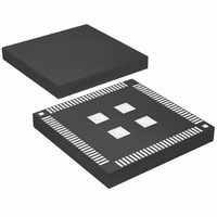
... AGND 23 AVDD 24 AGND ORDER PART NUMBER LTM2220IV-AA#PBF Consult LTC Marketing for parts specifi ed with wider operating temperature ranges. 2 Power Dissipation ............................................ 1500mW Operating Temperature Range ..................-40°C to 85°C Storage Temperature Range ....................-65°C to 125°C TOP VIEW AGND AGND AGND AGND SiPLGA PACKAGE 100-LEAD (16mm × ...
Page 3
CONVERTER CHARACTERISTICS temperature range, otherwise specifi cations are at T PARAMETER Resolution (No Missing Codes) Integral Linearity Error Differential Linearity Error Offset Error Gain Error ANALOG INPUTS The denotes the specifi cations which apply over the full operating temperature range, ...
Page 4
LTM2220-AA DIGITAL INPUTS AND OUTPUTS temperature range, otherwise specifi cations are at T SYMBOL PARAMETER CLOCK INPUTS (CLK+, CLK–) V Differential Input Voltage ID V Common Mode Input Voltage ICM R Input Resistance IN C Input Capacitance IN DIGITAL LOGIC ...
Page 5
TYPICAL PERFORMANCE CHARACTERISTICS 8192 Point FFT 5MHz, –1dB, IN 170Msps 0 –10 –20 –30 –40 –50 –60 –70 –80 –90 –100 –110 FREQUENCY (MHz) 2220 G01 8192 Point FFT, ...
Page 6
LTM2220-AA PIN FUNCTIONS NC (Pins 10, 11, 33, 42, 43, 44, 45, 46): Pin is not connected internally. AGND (Pins 4, 9, 12, 13, 16, 17, 20, 23, 25, 26, 30, 31, 32, 35, ...
Page 7
APPLICATIONS INFORMATION DYNAMIC PERFORMANCE Signal-to-Noise Plus Distortion Ratio The signal-to-noise plus distortion ratio [S/(N + D)] is the ratio between the RMS amplitude of the fundamen- tal input frequency and the RMS amplitude of all other frequency components at the ...
Page 8
LTM2220-AA APPLICATIONS INFORMATION SAMPLE/HOLD OPERATION AND INPUT DRIVE Sample/Hold Operation Figure 1 shows an equivalent circuit for the LTM2220-AA CMOS differential sample-and-hold. The analog inputs are AC coupled to the sample and hold circuit through 0.1µF capacitors and 1k bias ...
Page 9
APPLICATIONS INFORMATION Any noise present on the encode signal will result in ad- ditional aperture jitter that will be RMS summed with the inherent ADC aperture jitter. In applications where jitter is critical (high input frequen- cies) take the following ...
Page 10
LTM2220-AA APPLICATIONS INFORMATION DIGITAL OUTPUTS Table 1. Output Codes vs Input Voltage + – VIN – VIN OR >+0.768000V 1 +0.768000V 0 +0.767625V 0 +0.000375V 0 0.000000V 0 –0.000375V 0 –0.000750V 0 –0.767625V 0 –0.768000V 0 <–0.768000V 1 Digital Output ...
Page 11
... DETAIL A Information furnished by Linear Technology Corporation is believed to be accurate and reliable. However, no responsibility is assumed for its use. Linear Technology Corporation makes no representa- tion that the interconnection of its circuits as described herein will not infringe on existing patent rights. SiPLGA Package 100-Lead (16mm × 16mm) (Reference LTC DWG # 05-08-1802 Rev Ø ...
Page 12
... FAX: (408) 434-0507 ● COMMENTS 890mW, 67.7dB SNR, 84dB SFDR, 64-Pin QFN Package 740mW, 65.4dB SNR, 84dB SFDR, 64-Pin QFN Package 800MHz BW, 70dBc Distortion at 70MHz, 6dB Gain www.linear.com ● 2220aaf LT 0107 • PRINTED IN USA © LINEAR TECHNOLOGY CORPORATION 2007 ...