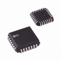
AD7828KP Analog Devices Inc, AD7828KP Datasheet - Page 10

AD7828KP
Manufacturer Part Number
AD7828KP
Description
IC ADC 8BIT LC2MOS 8CH 28-PLCC
Manufacturer
Analog Devices Inc
Datasheet
1.AD7828LRS-REEL.pdf
(16 pages)
Specifications of AD7828KP
Data Interface
Parallel
Rohs Status
RoHS non-compliant
Number Of Bits
8
Sampling Rate (per Second)
50k
Number Of Converters
3
Power Dissipation (max)
100mW
Voltage Supply Source
Single Supply
Operating Temperature
0°C ~ 70°C
Mounting Type
Surface Mount
Package / Case
28-LCC (J-Lead)
Resolution (bits)
8bit
Sampling Rate
50kSPS
Input Channel Type
Differential
Supply Voltage Range - Analog
4.75V To 5.25V
Supply Current
16mA
Digital Ic Case Style
LCC
Lead Free Status / RoHS Status
Contains lead / RoHS non-compliant
Available stocks
Company
Part Number
Manufacturer
Quantity
Price
Company:
Part Number:
AD7828KP
Manufacturer:
AD
Quantity:
1 010
Part Number:
AD7828KP
Manufacturer:
ADI/亚德诺
Quantity:
20 000
Company:
Part Number:
AD7828KP-REEL
Manufacturer:
Analog Devices Inc
Quantity:
10 000
Company:
Part Number:
AD7828KPZ
Manufacturer:
Analog Devices Inc
Quantity:
10 000
Part Number:
AD7828KPZ
Manufacturer:
ADI/亚德诺
Quantity:
20 000
AD7824/AD7828
MICROPROCESSOR INTERFACING
The AD7824/AD7828 is designed to interface to microprocessors
as Read Only Memory (ROM). Analog channel selection, con-
version start, and data read operations are controlled by CS, RD,
and the channel address inputs. These signals are common to
all memory peripheral devices.
Z80 MICROPROCESSOR
Figure 16 shows a typical AD7824/AD7828–Z80 interface. The
AD7824/AD7828 is operating in Mode 0. Assume the ADC is
assigned a memory block starting at address C000. The follow-
ing LOAD instruction to any of the addresses listed in Table II
will start a conversion of the selected channel and read the
conversion result.
At the beginning of the instruction cycle when the ADC
address is selected, RDY asserts the WAIT input so that the
Z80 is forced into a WAIT state. At the end of conversion,
RDY returns high and the conversion result is placed in the B
register of the microprocessor.
Address
C000
C001
C002
C003
C004
C005
C006
C007
MC68000 MICROPROCESSOR
Figure 17 shows an MC68000 interface. The AD7824/AD7828
is operating in Mode 0. Assume the ADC is again assigned a
memory block starting at address C000. A MOVE instruction
Z80
Figure 16. AD7824/AD7828–Z80 lnterface
MREQ
WAIT
Table II. Address Channel Selection
A15
RD
A0
D7
D0
**
*
LINEAR CIRCUITRY OMITTED FOR CLARITY.
FOR THE AD7828 ONLY
5V
5k
EN
LD B, (C000)
ADDRESS BUS
AD7824
Channel
1
2
3
4
DATA BUS
ADDRESS
DECODE
CS
RDY
RD
DB7
DB0
A0
A0
AD7824*
AD7828*
A1
A1
AD7828
Channel
1
2
3
4
5
6
7
8
A2
A2**
–10–
to any of the addresses in Table II starts a conversion and reads
the conversion result.
Once conversion has begun, the MC68000 inserts WAIT states
until INT goes low, asserting DTACK at the end of conversion.
The microprocessor then places the conversion results into the
D0 register.
TMS32010 MICROCOMPUTER
A TMS32010 interface is shown in Figure 18. The AD7824/
AD7828 is operating in Mode 1 (i.e., no µP WAIT states). The
ADC is mapped at a port address. The following I/O instruction
starts a conversion and reads the previous conversion result into
the accumulator.
The port address (000 to 111) selects the analog channel to be
converted. When conversion is complete, a second I/O instruc-
tion (IN, A PA) reads the up-to-date data into the accumulator
and starts another conversion. A delay of 2.5 µs must be allowed
between conversions.
Figure 18. AD7824/AD7828–TMS32010 Interface
Figure 17. AD7824/AD7828–MC68000 Interface
MC68000
TMS32010
DTACK
R/W
A23
IN, A PA (PA = PORT ADDRESS)
AS
A1
D7
D0
**
**
*
*
MEN
LINEAR CIRCUITRY OMITTED FOR CLARITY.
FOR THE AD7828 ONLY
DEN
LINEAR CIRCUITRY OMITTED FOR CLARITY.
FOR THE AD7828 ONLY
PA2
PA1
PA0
D7
D0
MOVE × B $C000, D0
Q
7474
EN
CLR
CK
ADDRESS BUS
DATA BUS
ADDRESS
D
DATA BUS
DECODE
5k
5V
A2**
A1
A0
CS
RD
DB7
DB0
CS
RD
RDY
DB7
DB0
AD7824*
AD7828*
A0
A0
AD7824*
AD7828*
A1
A1
A2
A2**
REV. F


