AD1674JNZ Analog Devices Inc, AD1674JNZ Datasheet
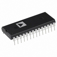
IC ADC 12BIT 100KSPS 28-DIP

AD1674JNZ

Manufacturer Part Number
AD1674JNZ
Description
IC ADC 12BIT 100KSPS 28-DIP
Manufacturer
Analog Devices Inc
Datasheet

Specifications of AD1674JNZ

Data Interface
Parallel
Number Of Bits
12
Sampling Rate (per Second)
100k
Number Of Converters
1
Power Dissipation (max)
825mW
Voltage Supply Source
Dual ±
Operating Temperature
0°C ~ 70°C
Mounting Type
Through Hole
Package / Case
28-DIP (0.600", 15.24mm)
Resolution (bits)
12bit
Sampling Rate
100kSPS
Input Channel Type
Single Ended
Supply Voltage Range - Digital
4.5V To 5.5V
Supply Current
14mA
Digital Ic Case Style
DIP
Lead Free Status / RoHS Status
Lead free / RoHS Compliant

Available stocks

Company
Part Number
Manufacturer
Quantity
Price
Part Number:
AD1674JNZ
Manufacturer:
ADI
Quantity:
76
Part Number:
AD1674JNZ
Manufacturer:
F
Quantity:
134
Part Number:
AD1674JNZ
Manufacturer:
ADI
Quantity:
3 244
Part Number:
AD1674JNZ
Manufacturer:
ADI
Quantity:
1 364
Part Number:
AD1674JNZ
Manufacturer:
ADI/亚德诺
Quantity:
20 000
a
PRODUCT DESCRIPTION
The AD1674 is a complete, multipurpose, 12-bit analog-to-
digital converter, consisting of a user-transparent onboard
sample-and-hold amplifier (SHA), 10 volt reference, clock and
three-state output buffers for microprocessor interface.
The AD1674 is pin compatible with the industry standard
AD574A and AD674A, but includes a sampling function while
delivering a faster conversion rate. The on-chip SHA has a wide
input bandwidth supporting 12-bit accuracy over the full
Nyquist bandwidth of the converter.
The AD1674 is fully specified for ac parameters (such as S/(N+D)
ratio, THD, and IMD) and dc parameters (offset, full-scale
error, etc.). With both ac and dc specifications, the AD1674 is
ideal for use in signal processing and traditional dc measure-
ment applications.
The AD1674 design is implemented using Analog Devices’
BiMOS II process allowing high performance bipolar analog cir-
cuitry to be combined on the same die with digital CMOS logic.
Five different temperature grades are available. The AD1674J
and K grades are specified for operation over the 0 C to +70 C
temperature range. The A and B grades are specified from
–40 C to +85 C; the AD1674T grade is specified from –55 C
to +125 C. The J and K grades are available in both 28-lead
plastic DIP and SOIC. The A and B grade devices are available
in 28-lead hermetically sealed ceramic DIP and 28-lead SOIC.
The T grade is available in 28-lead hermetically sealed ceramic
DIP.
*Protected by U. S. Patent Nos. 4,962,325; 4,250,445; 4,808,908; RE30586 .
REV. C
Information furnished by Analog Devices is believed to be accurate and
reliable. However, no responsibility is assumed by Analog Devices for its
use, nor for any infringements of patents or other rights of third parties
which may result from its use. No license is granted by implication or
otherwise under any patent or patent rights of Analog Devices.
FEATURES
Complete Monolithic 12-Bit 10 s Sampling ADC
On-Board Sample-and-Hold Amplifier
Industry Standard Pinout
8- and 16-Bit Microprocessor Interface
AC and DC Specified and Tested
Unipolar and Bipolar Inputs
Commercial, Industrial and Military Temperature
MIL-STD-883 and SMD Compliant Versions Available
5 V,
Range Grades
10 V, 0 V–10 V, 0 V–20 V Input Ranges
PRODUCT HIGHLIGHTS
1. Industry Standard Pinout: The AD1674 utilizes the pinout
2. Integrated SHA: The AD1674 has an integrated SHA which
3. DC and AC Specified: In addition to traditional dc specifica-
4. Analog Operation: The precision, laser-trimmed scaling and
5. Flexible Digital Interface: On-chip multiple-mode
One Technology Way, P.O. Box 9106, Norwood, MA 02062-9106, U.S.A.
Tel: 617/329-4700
established by the industry standard AD574A and AD674A.
supports the full Nyquist bandwidth of the converter. The
SHA function is transparent to the user; no wait-states are
needed for SHA acquisition.
tions, the AD1674 is also fully specified for frequency do-
main ac parameters such as total harmonic distortion,
signal-to-noise ratio and input bandwidth. These parameters
can be tested and guaranteed as a result of the onboard
SHA.
bipolar offset resistors provide four calibrated ranges:
0 V to +10 V and 0 V to +20 V unipolar, –5 V to +5 V and
–10 V to +10 V bipolar. The AD1674 operates on +5 V and
three-state output buffers and interface logic allow direct
connection to most microprocessors.
12 V or 15 V power supplies.
REF OUT
BIP OFF
REF IN
AGND
20V
10V
12/8
R/C
CS
CE
A
IN
IN
0
2.5k
FUNCTIONAL BLOCK DIAGRAM
2.5k
20k
5k
REF
10V
5k
SHA
10k
CLOCK
10k
5k
CONTROL
IDAC
COMP
12-Bit 100 kSPS
AD1674
SAR
DAC
A/D Converter
12
12
AD1674*
12
Fax: 617/326-8703
STS
DB11 (MSB)
DB0 (LSB)

Related parts for AD1674JNZ

AD1674JNZ Summary of contents

Page 1

FEATURES Complete Monolithic 12-Bit 10 s Sampling ADC On-Board Sample-and-Hold Amplifier Industry Standard Pinout 8- and 16-Bit Microprocessor Interface AC and DC Specified and Tested Unipolar and Bipolar Inputs V– V–20 V ...

Page 2

AD1674–SPECIFICATIONS ( MIN DC SPECIFICATIONS –12 V Parameter RESOLUTION INTEGRAL NONLINEARITY (INL) DIFFERENTIAL NONLINEARITY (DNL) (No Missing Codes) 1 UNIPOLAR OFFSET @ + BIPOLAR OFFSET @ + FULL-SCALE ERROR @ +25 C (with ...

Page 3

Parameter RESOLUTION INTEGRAL NONLINEARITY (INL) DIFFERENTIAL NONLINEARITY (DNL) (No Missing Codes) 1 UNIPOLAR OFFSET @ + BIPOLAR OFFSET @ + FULL-SCALE ERROR @ +25 C (with Fixed 50 Resistor from REF OUT to REF IN) ...

Page 4

AD1674–SPECIFICATIONS ( MIN AC SPECIFICATIONS –12 V Parameter Signal to Noise and Distortion (S/N+D) Ratio 4 Total Harmonic Distortion (THD) Peak Spurious or Peak Harmonic Component Full Power Bandwidth Full Linear Bandwidth 5 Intermodulation Distortion (IMD) Second Order ...

Page 5

SWITCHING SPECIFICATIONS CONVERTER START TIMING (Figure Grades Parameter Symbol Min Typ Max Conversion Time 8-Bit Cycle 12-Bit Cycle STS Delay from CE t DSC CE Pulse Width t 50 ...

Page 6

AD1674 TIMING—STAND-ALONE MODE (Figures 4a and 4b) Parameter Symbol Data Access Time t DDR Low R/C Pulse Width t HRL STS Delay from R Data Valid After R/C Low t HDR STS Delay After Data Valid t HS ...

Page 7

Symbol Pin No. Type Name and Function AGND 9 P Analog Ground (Common Byte Address/Short Cycle conversion is started with A 0 cycle is initiated results. During Read (R with 12/8 ...

Page 8

AD1674 DEFINITION OF SPECIFICATIONS INTEGRAL NONLINEARITY (INL) The ideal transfer function for an ADC is a straight line drawn between “zero” and “full scale.” The point used as “zero” occurs 1/2 LSB before the first code transition. “Full scale” is ...

Page 9

SAMPLE FULL-SCALE = +10V 0 –20 THD –40 –60 – HARMONIC –100 ND 2 HARMONIC –120 1 10 100 1000 10000 INPUT FREQUENCY – kHz Figure 5. Harmonic Distortion vs. Input Frequency 0 –20 –40 ...

Page 10

AD1674 12/8 FULL-CONTROL MODE Chip Enable (CE), Chip Select (CS) and Read/ Convert (R/C) are used to control Convert or Read modes of operation. Either may be used to initiate a conversion. ...

Page 11

R1 2 12/8 100k 3 CS –15V +15V R 100 100k 10 REF IN 100 8 REF OUT 12 BIP OFF AD1674 0 TO +10V 13 10V ANALOG IN INPUTS 14 20V IN ...

Page 12

AD1674 GROUNDING If a single AD1674 is used with separate analog and digital ground planes, connect the analog ground plane to AGND and the digital ground plane to DGND keeping lead lengths as short as possible. Then connect AGND and ...

Related keywords