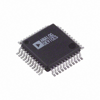
AD9240AS Analog Devices Inc, AD9240AS Datasheet

AD9240AS
Specifications of AD9240AS
Available stocks
Related parts for AD9240AS
AD9240AS Summary of contents
Page 1
FEATURES Monolithic 14-Bit, 10 MSPS A/D Converter Low Power Dissipation: 285 mW Single +5 V Supply Integral Nonlinearity Error: 2.5 LSB Differential Nonlinearity Error: 0.6 LSB Input Referred Noise: 0.36 LSB Complete: On-Chip Sample-and-Hold Amplifier and Voltage Reference Signal-to-Noise ...
Page 2
AD9240–SPECIFICATIONS (AVDD = +5 V, DVDD = +5 V, DRVDD = + SPECIFICATIONS MIN Parameter RESOLUTION MAX CONVERSION RATE INPUT REFERRED NOISE VREF = 1 V VREF = 2.5 V ACCURACY Integral Nonlinearity (INL) ...
Page 3
V, DVDD DRVDD = + SPECIFICATIONS AC Coupled/Differential Input, T Parameter SIGNAL-TO-NOISE AND DISTORTION RATIO (S/N+ 500 kHz INPUT f = 1.0 MHz INPUT f = 5.0 MHz INPUT EFFECTIVE ...
Page 4
AD9240 SWITCHING SPECIFICATIONS Parameters 1 Clock Period CLOCK Pulsewidth High CLOCK Pulsewidth Low Output Delay Pipeline Delay (Latency) NOTES 1 The clock period may be extended without degradation in specified performance @ +25 C. Specifications subject to ...
Page 5
PIN FUNCTION DESCRIPTIONS Pin Number Name Description 1 DVSS Digital Ground 2, 29 AVSS Analog Ground 3 DVDD +5 V Digital Supply 4, 28 AVDD +5 V Analog Supply 5 DRVSS Digital Output Driver Ground 6 DRVDD Digital Output Driver ...
Page 6
AD9240 Typical Differential AC Characterization Curves/Plots –0.5dBFS 75 –6.0dBFS 70 65 –20.0dBFS 0 INPUT FREQUENCY – MHz Figure 2. SINAD vs. Input Frequency (Input Span = 2.5 ...
Page 7
Other Characterization Curves/Plots 3.0 2.5 2.0 1.5 1.0 0.5 0.0 –0.5 –1.0 –1.5 –2.0 –2.5 –3.0 0 16863 CODE Figure 11. Typical INL (Input Span = –0.5dBFS 70 65 –6.0dBFS 60 55 –20.0dBFS 50 ...
Page 8
AD9240 INTRODUCTION The AD9240 uses a four-stage pipeline architecture with a wideband input sample-and-hold amplifier (SHA) implemented on a cost-effective CMOS process. Each stage of the pipeline, excluding the last, consists of a low resolution flash A/D con- nected to ...
Page 9
The addition of a differential input structure gives the user an additional level of flexibility that is not possible with traditional flash converters. The input stage allows the user to easily con- figure the inputs for either single-ended operation or ...
Page 10
AD9240 Figure 27 compares the AD9240’s THD vs. frequency perfor- mance for input span with a common-mode voltage and 2.5 V. Note the difference in the amount of degrada- tion in THD performance as ...
Page 11
Input Input Connection Coupling Span (V) VINA Single-Ended VREF VREF 2.5 – VREF 2.5 + VREF Single-Ended VREF ...
Page 12
AD9240 REFERENCE OPERATION The AD9240 contains an onboard bandgap reference that pro- vides a pin-strappable option to generate either 2.5 V output. With the addition of two external resistors, the user can generate reference voltages other ...
Page 13
DRIVING THE ANALOG INPUTS INTRODUCTION The AD9240 has a highly flexible input structure allowing it to interface with single-ended or differential input interface cir- cuitry. The applications shown in sections Driving the Analog Inputs and Reference Configurations, along with the ...
Page 14
AD9240 AC Coupling with Op Amps As previously stated, a dual op amp differential driver may be more suitable in applications in which the spectral content of the input signal falls below the cutoff frequency of a suitable RF transformer ...
Page 15
If the application requires the largest single-ended input range (i.e the AD9240, the op amp will require larger supplies to drive it. Various high speed amplifiers in the Op Amp Selection Guide of this ...
Page 16
AD9240 degrade slightly as the input common-mode voltage deviates from its optimum level of 2.5 V. Alternative AC Interface Figure 38 shows a flexible ac-coupled circuit which can be con- figured for different input spans. Since the common-mode voltage of ...
Page 17
VREF output is 2.5 V. The valid input range thus becomes The VREF pin should be bypassed to the REFCOM pin with tantalum capacitor in parallel with a low-inductance 0.1 ...
Page 18
AD9240 Variable Input Span with Figure 42 shows an example of the AD9240 configured for an input span of 2 VREF centered at 2 external 2.5 V reference drives the VINB pin thus ...
Page 19
Table V. Out-of-Range Truth Table OTR MSB Analog Input Range Range 1 0 Underrange 1 1 Overrange MSB OTR MSB Figure 46. Overrange or Underrange Logic Digital Output Driver Considerations (DRVDD) The AD9240 ...
Page 20
AD9240 Analog and Digital Supply Decoupling The AD9240 features separate analog and digital supply and ground pins, helping to minimize digital corruption of sensitive analog signals. 120 DVDD 100 AVDD 100 FREQUENCY – kHz Figure ...
Page 21
IF signal aliases back into the center of the ADC’s baseband region (i. sample rate of 10 MSPS image of the IF signal centered at 37.5 MHz will be aliased back to ...
Page 22
AD9240 AVSS1 AVSS2 AVDD1 AVDD2 DVDD DRVDD DVSS DRVSS Figure 55. Evaluation Board Schematic –22– SJ5 SJ4 SJ3 SJ2 SJ1 JG1 REV. B ...
Page 23
Figure 56. Evaluation Board Component Side Layout (Not to Scale) Figure 57. Evaluation Board Solder Side Layout (Not to Scale) B REV. Figure 58. Evaluation Board Ground Plane Layout (Not to Scale) Figure 59. Evaluation Board Power Plane Layout (Not ...
Page 24
... AD9240AS −55°C to +85°C AD9240ASRL −55°C to +85°C AD9240ASZ −55°C to +85°C AD9240ASZRL −55°C to +85° RoHS Compliant Part. ©2010 Analog Devices, Inc. All rights reserved. Trademarks and registered trademarks are the property of their respective owners. 1.03 2 ...


