KAD2708C-21Q68 Intersil, KAD2708C-21Q68 Datasheet
KAD2708C-21Q68
Specifications of KAD2708C-21Q68


Related parts for KAD2708C-21Q68


KAD2708C-21Q68 Summary of contents
Page 1
... VCM Ordering Information SPEED TEMP. PART NUMBER (MSPS) RANGE (°C) KAD2708C-27Q68 275 -40 to +85 KAD2708C-21Q68 210 -40 to +85 KAD2708C-17Q68 170 -40 to +85 KAD2708C-10Q68 105 -40 to +85 NOTES: 1. These Intersil Pb-free plastic packaged products employ special Pb- free material sets, molding compounds/die attach materials, and 100% ...
Page 2
... Typical Performance Curves ....................................... 9 Functional Description ................................................ 12 Reset ......................................................................... . 12 Voltage Reference ..................................................... . 12 Analog Input .............................................................. . 12 Clock Input ................................................................. . 13 Jitter ........................................................................... . 13 Digital Outputs ........................................................... . 14 Equivalent Circuits ....................................................... 14 Layout Considerations ................................................ 15 Split Ground and Power Planes ................................ . 15 Clock Input Considerations ........................................ . 15 Bypass and Filtering .................................................. . 15 LVCMOS Outputs ...................................................... . 15 Unused Inputs ........................................................... . 15 Definitions ..................................................................... 15 Package Outline Drawing ............................................ 16 2 KAD2708C FN6812.1 April 14, 2011 ...
Page 3
... 275MSPS, 210MSPS, 170MSPS and SAMPLE KAD2708C-17 KAD2708C-10 MAX MIN MAX MIN (Note 5) (Note 5) (Note 5) (Note 5) TYP 1.6 1.4 1.5 1.6 1.4 198 860 1.9 1.7 1.8 1.9 1.7 3.45 3.15 3.3 3 ...
Page 4
... MIN MAX (Note 6) TYP (Note 6) 0.8*AVDD3 0.2*AVDD3 0.8*AVDD3 0.2*AVDD3 0.8*OVDD2 0.2*OVDD2 KAD2708C-10 MAX (Note 5) TYP UNITS 50 MSPS ±0.2 0.4 LSB ±0.2 0.8 LSB 49.5 dBFS 49.2 dBFS 49.1 dBFS 49.5 dBFS 49.2 dBFS 48.9 dBFS 7.9 Bits 7.9 Bits 7 ...
Page 5
... CLKP, CLKN Differential Input Resistance CLKP, CLKN Common-Mode Input Voltage LVCMOS OUTPUTS Voltage Output High Voltage Output Low Output Rise Time Output Fall Time NOTE: 6. Compliance to datasheet limits is assured by one or more methods: production test, characterization and/or design. 5 KAD2708C CONDITIONS (Note 6) VIN = OVSS CDI R CDI V ...
Page 6
... Industry-standard protection techniques have been utilized in the design of this product. However, reasonable care must be taken in the storage and handling of ESD sensitive products. Contact Intersil for the specific ESD sensitivity rating of this product. 6 KAD2708C Sample PID ...
Page 7
... Exposed Paddle 7 KAD2708C NAME AVDD2 1.8V Analog Supply AVSS Analog Supply Return VREF Reference Voltage Out/In VREFSEL Reference Voltage Select (0:Int 1:Ext) VCM Common-Mode Voltage Output AVDD3 3.3V Analog Supply INP, INN Analog Input Positive, Negative DNC ...
Page 8
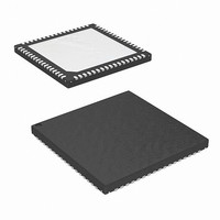
... Pin Configuration AVDD2 1 AVSS 2 VREF 3 VREFSEL 4 VCM 5 AVDD3 6 AVSS 7 INP 8 INN 9 AVSS 10 DNC 11 DNC 12 DNC 13 AVDD2 14 AVDD3 15 AVDD3 16 CLKDIV 17 8 KAD2708C KAD2708C 68 QFN Top View Not to Scale FIGURE 2. PIN CONFIGURATION 51 D4 DNC DNC DNC 45 OVSS 44 OVDD2 43 CLKOUT 42 DNC 41 OVDD2 DNC DNC 36 DNC ...
Page 9
... FIGURE 3. SNR AND SFDR SNR SFDR FIGURE 5. SNR AND SFDR SFDR SNR 100 150 200 (MSPS FIGURE 7. SNR AND SFDR KAD2708C AVDD2 = OVDD2 = 1.8V, AVDD3 = 3.3V -0.5dBFS unless noted. IN -50 -55 -60 -65 HD3 -70 -75 -80 HD2 -85 - -20 HD3 -30 -40 -50 HD2 -60 -70 -80 - -65 -70 -75 HD3 -80 -85 HD2 -90 ...
Page 10
... CODE FIGURE 11. INTEGRAL NONLINEARITY vs OUTPUT CODE 0 -20 -40 -60 -80 -100 -120 FREQUENCY (MHz) FIGURE 13. OUTPUT SPECTRUM @ 9.865MHz 10 KAD2708C AVDD2 = OVDD2 = 1.8V, AVDD3 = 3.3V -0.5dBFS unless noted. (Continued .75 0 .25 -0.5 -0 .75 -1 200 250 300 0 FIGURE 10. DIFFERENTIAL NONLINEARITY vs OUTPUT CODE SAMPLE 50,000 45,000 ...
Page 11
... FIGURE 17. TWO-TONE SPECTRUM @ 140MHz, 141MHz 75 70 SFDR SNR 40 -40 - AMBIENT TEMPERATURE, C FIGURE 19. SNR AND SFDR vs TEMPERATURE 11 KAD2708C AVDD2 = OVDD2 = 1.8V, AVDD3 = 3.3V -0.5dBFS unless noted. (Continued Ain = -0.48dBFS SNR = 49.3dBFS -20 SFDR = 63dBc SINAD = 49.1dBFS -40 HD2 = -63dBc HD3 = -67dBc -60 -80 -100 -120 ...
Page 12
... An external voltage may be applied to this pin to provide a more accurate reference than the internally generated bandgap voltage or to match the full-scale reference among a system of KAD2708C chips. One option in the latter configuration is to use one KAD2708C's internally generated reference as the external reference voltage for the other chips in the system ...
Page 13
... VCM Ω 25O 0.1µF Use of the clock divider is optional. The KAD2708C's ADC requires a clock with 50% duty cycle for optimum performance. If such a clock is not available, one option is to generate twice the desired sampling rate, then use the KAD2708C's divide-by-2 to generate a 50%-duty-cycle clock ...
Page 14
... F 2 Φ FIGURE 28. ANALOG INPUTS 14 KAD2708C Any internal aperture jitter combines with the input clock jitter root-sum-square fashion since they are not statistically correlated, and this determines the total jitter in 14 Bits the system. The total jitter, combined with other noise sources, then determines the achievable SNR ...
Page 15
... No license is granted by implication or otherwise under any patent or patent rights of Intersil or its subsidiaries. For information regarding Intersil Corporation and its products, see www.intersil.com 15 KAD2708C Clock Duty Cycle is the ratio of the time the clock wave is at logic high to the total time of one clock period. ...
Page 16
... Package Outline Drawing L68.10x10B 68 LEAD QUAD FLAT NO-LEAD PLASTIC PACKAGE Rev 0, 11/08 PIN 1 10.00 INDEX AREA 6 10.00 TOP VIEW 8.00 Sq 9.65 Sq 7.70 Sq TYPICAL RECOMMENDED LAND PATTERN 16 KAD2708C Exp. DAP 7.70 Sq. 35 (4X) 0.15 34 68X 0.55 BOTTOM VIEW 0.90 Max 64X 0.50 68X 0. ...