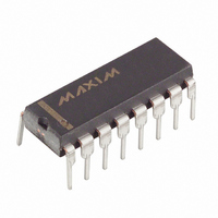
MAX1113EPE+ Maxim Integrated Products, MAX1113EPE+ Datasheet

MAX1113EPE+
Specifications of MAX1113EPE+
Related parts for MAX1113EPE+
MAX1113EPE+ Summary of contents
Page 1
... Pin Configurations appear at end of data sheet. SPI and QSPI are trademarks of Motorola, Inc. MICROWIRE is a trademark of National Semiconductor Corp. ________________________________________________________________ Maxim Integrated Products For free samples & the latest literature: http://www.maxim-ic.com, or phone 1-800-998-8800. For small orders, phone 1-800-835-8769. +5V, Low-Power, Multi-Channel, ...
Page 2
Low-Power, Multi-Channel, Serial 8-Bit ADCs ABSOLUTE MAXIMUM RATINGS V to AGND ..............................................................-0. AGND to DGND .......................................................-0.3V to 0.3V CH0–CH7, COM, REFIN, REFOUT to AGND ...................................-0. Digital Inputs to DGND ...............................................-0. Digital Outputs ...
Page 3
ELECTRICAL CHARACTERISTICS (continued +4.5V to +5.5V; unipolar input mode; COM = 0V cycle (50ksps); 1µF capacitor at REFOUT; T PARAMETER SYMBOL CONVERSION RATE Conversion Time (Note 4) Track/Hold Acquisition Time Aperture Delay Aperture Jitter Internal Clock ...
Page 4
Low-Power, Multi-Channel, Serial 8-Bit ADCs ELECTRICAL CHARACTERISTICS (continued +4.5V to +5.5V; unipolar input mode; COM = 0V cycle (50ksps); 1µF capacitor at REFOUT; T PARAMETER SYMBOL CS DIGITAL INPUTS: DIN, SCLK, DIN, SCLK, CS Input ...
Page 5
TIMING CHARACTERISTICS (Figures 8 and +4.5V to +5.5V MIN MAX PARAMETER SYMBOL Track/Hold Acquisition Time DIN to SCLK Setup DIN to SCLK Hold SCLK Fall to Output Data Valid CS ...
Page 6
Low-Power, Multi-Channel, Serial 8-Bit ADCs __________________________________________Typical Operating Characteristics (V = +5.0V 500kHz; external clock (50% duty cycle SCLK SUPPLY CURRENT vs. TEMPERATURE 180 OUTPUT CODE = FULL SCALE C = 10pF LOAD 160 V = ...
Page 7
PIN NAME MAX1112 MAX1113 1–4 1–4 CH0–CH3 5–8 — CH4–CH7 9 5 COM SHDN REFIN 12 8 REFOUT 13 9 AGND 14 10 DGND 15 11 DOUT 16 12 SSTRB 17 13 DIN ...
Page 8
Low-Power, Multi-Channel, Serial 8-Bit ADCs _______________Detailed Description The MAX1112/MAX1113 analog-to-digital converters (ADCs) use a successive-approximation conversion technique and input track/hold (T/H) circuitry to convert an analog signal to an 8-bit digital output. A flexible seri- al interface provides easy ...
Page 9
Table 1a. MAX1112 Channel Selection in Single-Ended Mode (SGL/DIF = 1) SEL2 SEL1 SEL0 CH0 ...
Page 10
Low-Power, Multi-Channel, Serial 8-Bit ADCs The time required for the T/H to acquire an input signal is a function of how quickly its input capacitance is charged. If the input signal’s source impedance is high, the acquisition time lengthens, ...
Page 11
Table 4. Full-Scale and Zero-Scale Voltages UNIPOLAR MODE Full Scale Zero Scale V + COM COM REFIN in control bytes of $FF (hex), which trigger single- ended, unipolar conversions on CH7 (MAX1112) or CH3 (MAX1113) in external clock mode without ...
Page 12
Low-Power, Multi-Channel, Serial 8-Bit ADCs I/O SCK MISO + SPI CS SCK MISO + QSPI I MICROWIRE Figure 6. Common Serial-Interface Connections to the MAX1112/MAX1113 SCLK SEL2 SEL1 SEL0 ...
Page 13
In unipolar input mode, the output is straight binary (Figure 15). For bipolar inputs, the output is two’s-com- plement (Figure 16). Data is clocked out at SCLK’s falling edge in MSB-first format. The MAX1112/MAX1113 can use either an external ser- ...
Page 14
Low-Power, Multi-Channel, Serial 8-Bit ADCs SCLK UNI/ SEL2 SEL1 SEL0 BIP DIN START SSTRB DOUT A/D STATE IDLE Figure 10. Internal Clock Mode Timing CS t CSH SSTRB SCLK PD0 CLOCK IN Figure ...
Page 15
CS 1 SCLK DIN S CONTROL BYTE 0 DOUT SSTRB Figure 12a. Continuous Conversions, External Clock Mode, 10 Clocks/Conversion Timing CS SCLK S CONTROL BYTE 0 DIN DOUT Figure 12b. Continuous Conversions, External Clock Mode, 16 Clocks/Conversion Timing The falling ...
Page 16
Low-Power, Multi-Channel, Serial 8-Bit ADCs __________Applications Information Power-On Reset When power is first applied, and if SHDN is not pulled low, internal power-on reset circuitry activates the MAX1112/MAX1113 in internal clock mode. SSTRB is high on power-up and, if ...
Page 17
CLOCK INTERNAL MODE SHDN SETS EXTERNAL CLOCK MODE DIN DATA VALID DOUT POWERED UP MODE Figure 14a. Power-Down Modes, External Clock Timing Diagram SETS INTERNAL CLOCK MODE ...
Page 18
Low-Power, Multi-Channel, Serial 8-Bit ADCs OUTPUT CODE FULL-SCALE TRANSITION 11111111 11111110 11111101 00000011 00000010 00000001 00000000 (COM) INPUT VOLTAGE (LSB) Figure 15. Unipolar Transfer Function OUTPUT CODE V REFIN + COM 2 01111111 ...
Page 19
TOP VIEW CH0 1 CH1 2 CH2 3 CH3 4 MAX1112 CH4 5 CH5 6 CH6 7 CH7 8 COM 9 SHDN 10 DIP/SSOP Ordering Information (continued) PART TEMP. RANGE MAX1112EPP -40°C to +85°C MAX1112EAP -40°C to +85°C MAX1112MJP -55°C ...
Page 20
... Maxim cannot assume responsibility for use of any circuitry other than circuitry entirely embodied in a Maxim product. No circuit patent licenses are implied. Maxim reserves the right to change the circuitry and specifications without notice at any time. 20 ____________________Maxim Integrated Products, 120 San Gabriel Drive, Sunnyvale, CA 94086 408-737-7600 © 1998 Maxim Integrated Products Printed USA ...


