MAX1274BETC+ Maxim Integrated Products, MAX1274BETC+ Datasheet - Page 8
MAX1274BETC+
Manufacturer Part Number
MAX1274BETC+
Description
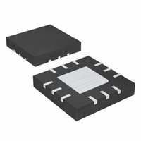
IC ADC 12BIT 1.8MSPS 12-TQFN
Manufacturer
Maxim Integrated Products
Datasheet
1.MAX1274BETCT.pdf
(18 pages)
Specifications of MAX1274BETC+
Number Of Bits
12
Sampling Rate (per Second)
1.8M
Data Interface
MICROWIRE™, QSPI™, Serial, SPI™
Number Of Converters
1
Power Dissipation (max)
45mW
Voltage Supply Source
Analog and Digital
Operating Temperature
-40°C ~ 85°C
Mounting Type
Surface Mount
Package / Case
12-WQFN Exposed Pad
Lead Free Status / RoHS Status
Lead free / RoHS Compliant


1.8Msps, Single-Supply, Low-Power,
True-Differential, 12-Bit ADCs
(V
at T
8
DD
A
_______________________________________________________________________________________
5, 11
= +5V, V
PIN
= +25°C)
10
12
—
1
2
3
4
6
7
8
9
L
= V
CNVST
NAME
RGND
DOUT
DD
SCLK
AIN+
GND
AIN-
N.C.
V
REF
V
EP
DD
, V
L
1.0
0.8
0.6
0.4
0.2
REF
0
-40
= 4.096V, f
Negative Analog Input
External Reference Voltage Input. V
capacitor and a 4.7µF capacitor to RGND.
Reference Ground. Connect RGND to GND.
Positive Analog Supply Voltage (+4.75V to +5.25V). Bypass V
capacitor to GND.
No Connection
Ground. GND is internally connected to EP.
Positive Logic Supply Voltage (1.8V to V
to GND.
Serial Data Output. Data is clocked out on the rising edge of SCLK.
Convert Start. Forcing CNVST high prepares the part for a conversion. Conversion begins on the
falling edge of CNVST. The sampling instant is defined by the falling edge of CNVST.
Serial Clock Input. Clocks data out of the serial interface. SCLK also sets the conversion speed.
Positive Analog Input
Exposed Paddle. EP is internally connected to GND.
-15
V
vs. TEMPERATURE
L
TEMPERATURE (°C)
SUPPLY CURRENT
10
SCLK
CONVERTING
f
SCLK
FULL/PARTIAL
POWER-DOWN
f
SCLK
= 28.8MHz
= 28.8MHz, T
35
= 28.8MHz
Typical Operating Characteristics (continued)
60
A
85
= -40°C to +85°C, unless otherwise noted. Typical values are measured
REF
sets the analog input range. Bypass REF with a 0.01µF
DD
1.0
0.8
0.5
0.3
). Bypass V
0
FUNCTION
0
vs. CONVERSION RATE
500
V
L
L
with a 0.01µF capacitor and a 10µF capacitor
SUPPLY CURRENT
f
SAMPLE
1000
DD
V
L
(kHz)
V
= 3V
L
with a 0.01µF capacitor and a 10µF
= 5V
1500
V
L
= 1.8V
Pin Description
2000
Related parts for MAX1274BETC+
Image
Part Number
Description
Manufacturer
Datasheet
Request
R

Part Number:
Description:
(MAX1274 / MAX1275) 12-Bit ADCs
Manufacturer:
Maxim Integrated Products
Datasheet:
Part Number:
Description:
MAX7528KCWPMaxim Integrated Products [CMOS Dual 8-Bit Buffered Multiplying DACs]
Manufacturer:
Maxim Integrated Products
Datasheet:
Part Number:
Description:
Single +5V, fully integrated, 1.25Gbps laser diode driver.
Manufacturer:
Maxim Integrated Products
Datasheet:
Part Number:
Description:
Single +5V, fully integrated, 155Mbps laser diode driver.
Manufacturer:
Maxim Integrated Products
Datasheet:
Part Number:
Description:
VRD11/VRD10, K8 Rev F 2/3/4-Phase PWM Controllers with Integrated Dual MOSFET Drivers
Manufacturer:
Maxim Integrated Products
Datasheet:
Part Number:
Description:
Highly Integrated Level 2 SMBus Battery Chargers
Manufacturer:
Maxim Integrated Products
Datasheet:
Part Number:
Description:
Current Monitor and Accumulator with Integrated Sense Resistor; ; Temperature Range: -40°C to +85°C
Manufacturer:
Maxim Integrated Products
Part Number:
Description:
TSSOP 14/A�/RS-485 Transceivers with Integrated 100O/120O Termination Resis
Manufacturer:
Maxim Integrated Products
Part Number:
Description:
TSSOP 14/A�/RS-485 Transceivers with Integrated 100O/120O Termination Resis
Manufacturer:
Maxim Integrated Products
Part Number:
Description:
QFN 16/A�/AC-DC and DC-DC Peak-Current-Mode Converters with Integrated Step
Manufacturer:
Maxim Integrated Products
Part Number:
Description:
TDFN/A/65V, 1A, 600KHZ, SYNCHRONOUS STEP-DOWN REGULATOR WITH INTEGRATED SWI
Manufacturer:
Maxim Integrated Products
Part Number:
Description:
Integrated Temperature Controller f
Manufacturer:
Maxim Integrated Products
Part Number:
Description:
SOT23-6/I�/45MHz to 650MHz, Integrated IF VCOs with Differential Output
Manufacturer:
Maxim Integrated Products
Part Number:
Description:
SOT23-6/I�/45MHz to 650MHz, Integrated IF VCOs with Differential Output
Manufacturer:
Maxim Integrated Products
Part Number:
Description:
EVALUATION KIT/2.4GHZ TO 2.5GHZ 802.11G/B RF TRANSCEIVER WITH INTEGRATED PA
Manufacturer:
Maxim Integrated Products