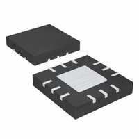
MAX1274BETC+ Maxim Integrated Products, MAX1274BETC+ Datasheet - Page 9

MAX1274BETC+
Manufacturer Part Number
MAX1274BETC+
Description
IC ADC 12BIT 1.8MSPS 12-TQFN
Manufacturer
Maxim Integrated Products
Datasheet
1.MAX1274BETCT.pdf
(18 pages)
Specifications of MAX1274BETC+
Number Of Bits
12
Sampling Rate (per Second)
1.8M
Data Interface
MICROWIRE™, QSPI™, Serial, SPI™
Number Of Converters
1
Power Dissipation (max)
45mW
Voltage Supply Source
Analog and Digital
Operating Temperature
-40°C ~ 85°C
Mounting Type
Surface Mount
Package / Case
12-WQFN Exposed Pad
Lead Free Status / RoHS Status
Lead free / RoHS Compliant
Figure 3. Functional Diagram
The MAX1274/MAX1275 use an input T/H and succes-
sive-approximation register (SAR) circuitry to convert
an analog input signal to a digital 12-bit output. The
serial interface requires only three digital lines (SCLK,
CNVST, and DOUT) and provides easy interfacing to
microprocessors (µPs) and DSPs. Figure 3 shows the
simplified internal structure for the MAX1274/MAX1275.
The equivalent circuit of Figure 4 shows the input archi-
tecture of the MAX1274/MAX1275, which is composed
of a T/H, a comparator, and a switched-capacitor digi-
tal-to-analog converter (DAC). The T/H enters its track-
ing mode on the 14th SCLK rising edge of the previous
conversion. Upon power-up, the T/H enters its tracking
mode immediately. The positive input capacitor is con-
nected to AIN+. The negative input capacitor is con-
nected to AIN-. The T/H enters its hold mode on the
falling edge of CNVST and the difference between the
sampled positive and negative input voltages is con-
verted. The time required for the T/H to acquire an input
signal is determined by how quickly its input capaci-
tance is charged. If the input signal’s source imped-
ance is high, the acquisition time lengthens. The
acquisition time, t
AIN+
AIN-
REF
True-Differential Analog Input T/H
T/H
MAX1275
MAX1274
ACQ
_______________________________________________________________________________________
, is the minimum time needed for
Detailed Description
12-BIT
SAR
ADC
V
DD
RGND
1.8Msps, Single-Supply, Low-Power,
LOGIC AND
CONTROL
TIMING
OUTPUT
BUFFER
GND
V
L
True-Differential, 12-Bit ADCs
DOUT
CNVST
SCLK
the signal to be acquired. It is calculated by the follow-
ing equation:
where R
the input signal.
Note: t
impedance below 12Ω does not significantly affect the
ADC’s AC performance.
The ADC’s input-tracking circuitry has a 20MHz small-
signal bandwidth, making it is possible to digitize high-
speed transient events and measure periodic
signals with bandwidths exceeding the ADC’s sam-
pling rate by using undersampling techniques. To
avoid high-frequency signals being aliased into the fre-
quency band of interest, anti-alias filtering is recom-
mended.
Internal protection diodes that clamp the analog input
to V
from GND - 0.3V to V
inputs must not exceed V
accurate conversions.
Figure 4. Equivalent Input Circuit
AIN+
AIN+
AIN-
AIN-
DD
ACQ
and GND allow the analog input pins to swing
IN
= 200Ω, and RS is the source impedance of
C
C
C
C
IN+
IN+
is never less than 104ns and any source
IN-
IN-
t
ACQ
R
R
R
R
IN+
IN+
IN-
IN-
≥ 9 × (RS + R
HOLD/CONVERSION MODE
DD
ACQUISITION MODE
Analog Input Protection
+ 0.3V without damage. Both
V
V
DD
AZ
AZ
or be lower than GND for
IN
COMP
COMP
) × 16pF
Input Bandwidth
CAPACITIVE
CAPACITIVE
CONTROL
CONTROL
LOGIC
LOGIC
DAC
DAC
9


