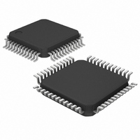
MAX1304ECM+T Maxim Integrated Products, MAX1304ECM+T Datasheet - Page 13

MAX1304ECM+T
Manufacturer Part Number
MAX1304ECM+T
Description
IC ADC 12BIT 8CH 4MSPS 48LQFP
Manufacturer
Maxim Integrated Products
Datasheet
1.MAX1304ECM.pdf
(37 pages)
Specifications of MAX1304ECM+T
Number Of Bits
12
Sampling Rate (per Second)
3.65M
Data Interface
Parallel
Number Of Converters
1
Power Dissipation (max)
1.82W
Voltage Supply Source
Analog and Digital
Operating Temperature
-40°C ~ 85°C
Mounting Type
Surface Mount
Package / Case
48-LQFP
Lead Free Status / RoHS Status
Lead free / RoHS Compliant
8-/4-/2-Channel, 12-Bit, Simultaneous-Sampling ADCs
MAX1304
MAX1308
MAX1312
1, 15, 17
2, 3, 14,
16, 23
with ±10V, ±5V, and 0 to +5V Analog Input Ranges
10
11
12
13
18
19
4
5
6
7
8
9
MAX1305
MAX1309
MAX1313
1, 15, 17
2, 3, 14,
16, 23
PIN
—
—
—
—
13
18
19
4
5
6
7
8
______________________________________________________________________________________
MAX1306
MAX1310
MAX1314
1, 15, 17
2, 3, 14,
16, 23
13
18
19
—
—
—
—
—
—
4
5
6
INTCLK/
REF
NAME
AGND
AV
CH0
CH1
MSV
CH2
CH3
CH4
CH5
CH6
CH7
REF
DD
MS
Analog Power Input. AV
converter. Apply +5V to AV
Layout, Grounding, and Bypassing section for additional information.
Analog Ground. AGND is the power return for AV
pins together.
Channel 0 Analog Input
Channel 1 Analog Input
Midscale Voltage Bypass. For the unipolar MAX1304/MAX1305/MAX1306,
connect a 2.2µF and a 0.1µF capacitor from MSV to AGND. For the bipolar
MAX1308/MAX1309/MAX1310/MAX1312/MAX1313/MAX1314, connect
MSV to AGND.
Channel 2 Analog Input
Channel 3 Analog Input
Channel 4 Analog Input
Channel 5 Analog Input
Channel 6 Analog Input
Channel 7 Analog Input
Clock-Mode Select Input. Connect INTCLK/
internal clock. Connect INTCLK/
connected to CLK.
Midscale Reference Bypass or Input. REF
to the internal +2.5V bandgap reference buffer.
For the MAX1304/MAX1305/MAX1306 unipolar devices, V
to the unity-gain buffer that drives MSV. MSV sets the midpoint of the input
voltage range. For internal reference operation, bypass REF
capacitor to AGND. For external reference operation, drive REF
external voltage from +2V to +3V.
For the MAX1308/MAX1309/MAX1310/MAX1312/MAX1313/MAX1314 bipolar
devices, connect REF
REF
operation, drive the REF
ADC Reference Bypass or Input. REF connects through a 5k resistor to the
internal +2.5V bandgap reference buffer.
For internal reference operation, bypass REF with a 0.01µF capacitor.
For external reference operation with the MAX1304/MAX1305/MAX1306
unipolar devices, drive REF with an external voltage from +2V to +3V.
For external reference operation with the MAX1308/MAX1309/MAX1310/
MAX1312/MAX1313/MAX1314 bipolar devices, connect REF
drive the REF
MS
/REF node with a 0.01µF capacitor to AGND. For external reference
MS
/REF node with an external voltage from +2V to +3V.
MS
MS
DD
to REF. For internal reference operation, bypass the
/REF node with an external voltage from +2V to +3V.
is the power input for the analog section of the
DD
. Connect all AV
FUNCTION
to AGND to use an external clock
MS
connects through a 5k
DD
DD
pins together. See the
. Connect all AGND
Pin Description
to AV
DD
REFMS
MS
MS
to select the
MS
with a 0.01µF
to REF and
is the input
with an
resistor
13


