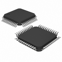
MAX1304ECM+T Maxim Integrated Products, MAX1304ECM+T Datasheet - Page 33

MAX1304ECM+T
Manufacturer Part Number
MAX1304ECM+T
Description
IC ADC 12BIT 8CH 4MSPS 48LQFP
Manufacturer
Maxim Integrated Products
Datasheet
1.MAX1304ECM.pdf
(37 pages)
Specifications of MAX1304ECM+T
Number Of Bits
12
Sampling Rate (per Second)
3.65M
Data Interface
Parallel
Number Of Converters
1
Power Dissipation (max)
1.82W
Voltage Supply Source
Analog and Digital
Operating Temperature
-40°C ~ 85°C
Mounting Type
Surface Mount
Package / Case
48-LQFP
Lead Free Status / RoHS Status
Lead free / RoHS Compliant
8-/4-/2-Channel, 12-Bit, Simultaneous-Sampling ADCs
Gain error is a figure of merit that indicates how well the
slope of the actual transfer function matches the slope
of the ideal transfer function. For the MAX1304–
MAX1306/MAX1308–MAX1310/MAX1312–MAX1314, the
gain error is the difference of the measured full-scale
and zero-scale transition points minus the difference of
the ideal full-scale and zero-scale transition points.
For the unipolar devices (MAX1304/MAX1305/
MAX1306), the full-scale transition point is from 0xFFE
to 0xFFF and the zero-scale transition point is from
0x000 to 0x001.
For the bipolar devices (MAX1308/MAX1309/MAX1310/
MAX1312/MAX1313/MAX1314), the full-scale transition
point is from 0x7FE to 0x7FF and the zero-scale transi-
tion point is from 0x800 to 0x801.
For a waveform perfectly reconstructed from digital
samples, the theoretical maximum SNR is the ratio of
the full-scale analog input (RMS value) to the RMS
quantization error (residual error). The ideal, theoretical
minimum analog-to-digital noise is caused by quantiza-
tion error only and results directly from the ADC’s reso-
lution (N bits):
In reality, there are other noise sources such as thermal
noise, reference noise, and clock jitter.
For these devices, SNR is computed by taking the ratio
of the RMS signal to the RMS noise. RMS noise
includes all spectral components to the Nyquist fre-
quency excluding the fundamental, the first five har-
monics, and the DC offset.
SINAD is computed by taking the ratio of the RMS signal
to the RMS noise plus distortion. RMS noise plus distor-
tion includes all spectral components to the Nyquist fre-
quency excluding the fundamental and the DC offset.
SINAD dB
with ±10V, ±5V, and 0 to +5V Analog Input Ranges
Signal-to-Noise Plus Distortion (SINAD)
(
SNR
)
=
20
dB[max]
x
______________________________________________________________________________________
log
Signal-to-Noise Ratio (SNR)
= 6.02
⎛
⎜
⎝
(
NOISE
dB
× N + 1.76
SIGNAL
+
DISTORTION
RMS
Gain Error
dB
)
RMS
⎞
⎟
⎠
ENOB specifies the dynamic performance of an ADC at
a specific input frequency and sampling rate. An ideal
ADC’s error consists of quantization noise only. ENOB for
a full-scale sinusoidal input waveform is computed as:
THD is the ratio of the RMS sum of the first five harmon-
ics to the fundamental itself. This is expressed as:
where V
V
order harmonics.
SFDR is the ratio of the RMS amplitude of the fundamen-
tal (maximum signal component) to the RMS value of the
next largest spurious component, excluding DC offset.
SFDR is specified in decibels relative to the carrier (dBc).
Channel-to-channel isolation indicates how well each
analog input is isolated from the others. The channel-to-
channel isolation for these devices is measured by
applying DC to channel 1 through channel 7 while an
AC 500kHz, -0.4dBFS sine wave is applied to channel
0. An FFT is taken for channel 0 and channel 1 and the
difference (in dB) of the 500kHz magnitudes is reported
as the channel-to-channel isolation.
Aperture delay (t
rising edge to the instant when an actual sample is taken.
6
THD
are the amplitudes of the 2nd- through 6th-
=
Spurious-Free Dynamic Range (SFDR)
1
20
is the fundamental amplitude, and V
x
Effective Number of Bits (ENOB)
Total Harmonic Distortion (THD)
log
ENOB
AD
⎛
⎜
⎜
⎝
Channel-to-Channel Isolation
) is the time delay from the CONVST
V
2 2
=
SINAD
+
V
3
6 02
2
.
+
−
V
V
1 76
Aperature Delay
.
4
1
2
+
V
5
2
+
2
V
through
6
2
⎞
⎟
⎟
⎠
33


