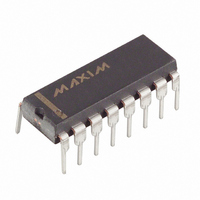
MAX194BCPE+ Maxim Integrated Products, MAX194BCPE+ Datasheet

MAX194BCPE+
Specifications of MAX194BCPE+
Related parts for MAX194BCPE+
MAX194BCPE+ Summary of contents
Page 1
... DGND 6 EOC DIP/Wide SO/Ceramic SB ________________________________________________________________ Maxim Integrated Products For free samples & the latest literature: http://www.maxim-ic.com, or phone 1-800-998-8800. For small orders, phone 408-737-7600 ext. 3468. ____________________________Features True 14-Bit Accuracy: 9.4µs Conversion Time 10µA Shutdown Mode Built-In Track/Hold AC and DC Specified ...
Page 2
ADC with 10µA Shutdown ABSOLUTE MAXIMUM RATINGS VDDD to DGND .....................................................................+7V VDDA to AGND......................................................................+7V VSSD to DGND.........................................................+0.3V to -6V VSSA to AGND .........................................................+0.3V to -6V VDDD to VDDA, VSSD to VSSA ..........................................±0.3V AIN, REF ....................................(VSSA - 0.3V) to ...
Page 3
ADC with 10µA Shutdown ELECTRICAL CHARACTERISTICS (continued) (VDDD = VDDA = +5V, VSSD = VSSA = -5V, f values are +25°C.) A PARAMETER SYMBOL DIGITAL INPUTS (CLK, CS, CONV, RESET, SCLK, BP/UP/SHDN) CLK, CS, CONV, ...
Page 4
ADC with 10µA Shutdown ELECTRICAL CHARACTERISTICS (continued) (VDDD = VDDA = +5V, VSSD = VSSA = -5V, f values are +25°C.) A PARAMETER SYMBOL POWER REQUIREMENTS (cont.) Power Dissipation VDDD Shutdown Supply Current I DDD ...
Page 5
ADC with 10µA Shutdown ______________________________________________________________Pin Description PIN NAME Bipolar/Unipolar/Shutdown Input. Three-state input selects bipolar or unipolar input range, or shutdown. 1 BP/UP/SHDN 0V = shutdown, +5V = unipolar, floating = bipolar. 2 CLK Conversion Clock Input 3 SCLK ...
Page 6
ADC with 10µA Shutdown MSB 32,768C 16,384C AIN REF AGND Figure 1. Capacitor DAC Functional Diagram CLK t RCH RESET EOC MAX194 OPERATION HALTS Figure 2. Initiating Calibration In an ideal DAC, each of the capacitors associated with ...
Page 7
ADC with 10µA Shutdown CLK EOC CONV TRACK/HOLD CONVERSION ENDS Figure 3. Initiating Conversions—At least 3 CLK cycles since end of previous conversion. If the power supplies do not settle within the MAX194’s power-on delay (500ns minimum), power-up ...
Page 8
ADC with 10µA Shutdown t CC1 CLK EOC CONV TRACK/HOLD CONVERSION ENDS Figure 4. Initiating Conversions—Less than 3 CLK cycles since end of previous conversion. sion and EOC will go high on the following CLK falling edge (Figure ...
Page 9
ADC with 10µA Shutdown START START CLK CONV Figure 5. Gating CONV to Synchronize with CLK CS CONV t CW CLK (CASE 1) CLK (CASE 2) EOC t DV B13 FROM PREVIOUS DOUT CONVERSION CONVERSION BEGINS CASE 1: ...
Page 10
ADC with 10µA Shutdown t CONV EOC t CSS CS SCLK (CASE 1) SCLK (CASE 2) SCLK (CASE 3) DOUT B13 MSB t DV CASE 1: SCLK IDLES LOW, DATA LATCHED ON RISING EDGE (CPOL = 0, CPHA ...
Page 11
ADC with 10µA Shutdown Table 1. Low-ESR Capacitor Suppliers COMPANY Sprague AVX Sanyo Nichicon BRIDGE Figure 9. Ratiometric Measurement Without an Accurate Reference __________Applications Information The MAX194 reference voltage range VDDA. When choosing the reference ...
Page 12
ADC with 10µA Shutdown +15V 0 MAX874 8 COMP 1000pF 4.096V 6 V OUT GND 4 Figure 10. Typical Reference Circuit for AC Accuracy 2 Figure 11. ...
Page 13
ADC with 10µA Shutdown INPUT SIGNAL Figure 12. Analog Input Protection for Overvoltage or Improper Supply Sequence IN1 IN2 IN3 IN4 CLK EOC A0 A1 Figure 13. Change multiplexer input near beginning of conversion to allow time for ...
Page 14
ADC with 10µA Shutdown +15V 2 7 MAX400 -15V Figure 14. MAX400 Drives AIN for Low-Frequency Use +15V 0 MAX427 0.1 F -15V Figure 15. AIN Buffer for ...
Page 15
ADC with 10µA Shutdown Figure 16. ±5V Buffer for AC/DC Use Has ±3.5V Swing Input Acquisition and Settling Four conversion-clock periods are allocated for acquir- ing the input signal. At the highest conversion rate, four clock periods is ...
Page 16
ADC with 10µA Shutdown QSPI PCS0 SCK MISO GPT *OC3 *IC1 *OC2 * THE USE OF THESE SIGNALS ADDS FLEXIBILITY AND FUNCTIONALITY BUT IS NOT REQUIRED TO IMPLEMENT THE INTERFACE. Figure 17. MAX194 Connection to QSPI Processor Clocking ...
Page 17
ADC with 10µA Shutdown CS, CONV CLK EOC B13 FROM PREVIOUS DOUT CONVERSION t DV DATA LATCHED: Figure 18. Timing Diagram for Circuit of Figure 17 QSPI PCS0 SCK MISO OC3 GPT IC1 OC2 IC3 74HC32 1.3 s ...
Page 18
ADC with 10µA Shutdown 588ns CLK START EOC CS SCLK DOUT 1.3 s Figure 20. Timing Diagram for Circuit of Figure 19 Complete source code for the Motorola 68HC16 and the MAX194 evaluation kit (EV kit) using this ...
Page 19
ADC with 10µA Shutdown Figure 21. MAX194 Code Listing for 68HC16 Module and Circuit of Figure 19 ______________________________________________________________________________________ 19 ...
Page 20
ADC with 10µA Shutdown Figure 21. MAX194 Code Listing for 68HC16 Module and Circuit of Figure 19 (continued) 20 ______________________________________________________________________________________ ...
Page 21
ADC with 10µA Shutdown Figure 21. MAX194 Code Listing for 68HC16 Module and Circuit of Figure 19 (continued) Constraints on sequencing the four power supplies are as follows. • Apply VDDA before VDDD. • Apply VSSA before VSSD. ...
Page 22
ADC with 10µA Shutdown 0 0 Figure 22. Supply Bypassing and Grounding graph of theoretical power consumption vs. conver- sions ...
Page 23
ADC with 10µA Shutdown + CLK CLOCK SHUTDOWN CLK) Q (CLK) J (CLOCK SHUTDOWN) Figure 24. Circuit to Stop Free-Running Asynchronous CLK -10 -30 -50 -70 -90 -110 -130 -150 ...
Page 24
... Maxim cannot assume responsibility for use of any circuitry other than circuitry entirely embodied in a Maxim product. No circuit patent licenses are implied. Maxim reserves the right to change the circuitry and specifications without notice at any time. 24 ____________________Maxim Integrated Products, 120 San Gabriel Drive, Sunnyvale, CA 94086 408-737-7600 © 1997 Maxim Integrated Products 90 ...


