AD9040AJR Analog Devices Inc, AD9040AJR Datasheet
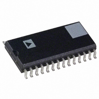
IC ADC 10BIT 40MSPS 28-SOIC

AD9040AJR

Manufacturer Part Number
AD9040AJR
Description
IC ADC 10BIT 40MSPS 28-SOIC
Manufacturer
Analog Devices Inc
Datasheet

Specifications of AD9040AJR

Rohs Status
RoHS non-compliant
Number Of Bits
10
Sampling Rate (per Second)
40M
Data Interface
Parallel
Number Of Converters
2
Power Dissipation (max)
1.2W
Voltage Supply Source
Analog and Digital, Dual ±
Operating Temperature
0°C ~ 70°C
Mounting Type
Surface Mount
Package / Case
28-SOIC (0.300", 7.50mm Width)

Available stocks

Company
Part Number
Manufacturer
Quantity
Price
Part Number:
AD9040AJR
Quantity:
5 510
Part Number:
AD9040AJR
Manufacturer:
AD
Quantity:
283
Part Number:
AD9040AJR
Manufacturer:
ADI
Quantity:
218
Part Number:
AD9040AJR
Manufacturer:
AD
Quantity:
1 000
Part Number:
AD9040AJR
Manufacturer:
ADI/亚德诺
Quantity:
20 000
Part Number:
AD9040AJRZ
Manufacturer:
ADI/亚德诺
Quantity:
20 000
GENERAL DESCRIPTION
The AD9040A is a complete 10-bit monolithic sampling analog-
to-digital converter (ADC) with on-board track-and-hold (T/H)
and reference. The unit is designed for low cost, high perfor-
mance applications and requires only an encode signal to achieve
40 MSPS sample rates with 10-bit resolution.
Digital inputs and outputs are CMOS compatible; the analog
input requires a signal of 2 V p-p amplitude. The two-step
architecture used in the AD9040A is optimized to provide the
best dynamic performance available while maintaining low
power requirements of only 940 mW typically; maximum dissi-
pation is 1.1 W at 40 MSPS.
The signal-to-noise ratio (SNR), including harmonics, is 53 dB,
or 8.5 ENOB, when sampling an analog input of 10.3 MHz at
40 MSPS. Competitive devices perform at less than 7.5 ENOB
and require external references and larger input signals.
The AD9040A A/D converter is available in either a 28-lead
PDIP or a 28-lead SOIC package. The two models operate over
a commercial temperature range of 0°C to 70°C. Contact the
factory regarding availability of ceramic military temperature
range devices.
REV. D
Information furnished by Analog Devices is believed to be accurate and
reliable. However, no responsibility is assumed by Analog Devices for its
use, nor for any infringements of patents or other rights of third parties that
may result from its use. No license is granted by implication or otherwise
under any patent or patent rights of Analog Devices. Trademarks and
registered trademarks are the property of their respective companies.
FEATURES
Low Power: 940 mW
53 dB SNR @ 10 MHz A
On-Chip Track-and-Hold, Reference
CMOS Compatible
2 V p-p Analog Input
Fully Characterized Dynamic Performance
APPLICATIONS
Ultrasound Medical Imaging
Digital Oscilloscopes
Professional Video
Digital Communications
Advanced Television (MUSE Decoders)
Instrumentation
IN
PRODUCT HIGHLIGHTS
1. CMOS compatible logic for direct interface to ASICs.
2. On-board track-and-hold provides excellent high frequency
3. High input impedance and 2 V p-p input range reduce need
4. Easy to use; no cumbersome external voltage references
5. Available in 28-lead PDIP and SOIC packages.
6. Evaluation board includes AD9040AJR, reconstruction DAC,
One Technology Way, P.O. Box 9106, Norwood, MA 02062-9106, U.S.A.
Tel: 781/329-4700
Fax: 781/326-8703
GND
BP
performance on analog inputs, critical for communications
and medical imaging applications.
for external amplifiers.
required, allowing denser packing of ADCs for multichannel
applications.
and latches. Space is available near the analog input and digital
outputs of the converter for additional circuits. Order as part
number AD9040A/PCB (schematic shown in data sheet).
V
V
OUT
A
REF
REF
IN
REFERENCE
BAND GAP
AD9040A
FUNCTIONAL BLOCK DIAGRAM
ENCODE
AMP
REF
T/H
© 2003 Analog Devices, Inc. All rights reserved.
5-BIT
ADC
DECODE
LOGIC
T/H
10-Bit 40 MSPS
A/D Converter
CORRECTION
ERROR
T/H
AD9040A
ARRAY
AMP
6-BIT
www.analog.com
ADC
DECODE
LOGIC
10

Related parts for AD9040AJR

AD9040AJR Summary of contents

Page 1

... ADCs for multichannel applications. 5. Available in 28-lead PDIP and SOIC packages. 6. Evaluation board includes AD9040AJR, reconstruction DAC, and latches. Space is available near the analog input and digital outputs of the converter for additional circuits. Order as part number AD9040A/PCB (schematic shown in data sheet). ...

Page 2

... Third Harmonic Distortion f = 2.3 MHz 10.3 MHz IN 6 Two-Tone Intermodulation Distortion Rejections Differential Phase Differential Gain (+ –V = –5 V; internal reference: Encode = 40.5 MSPS, unless otherwise noted.) Test AD9040AJN/AD9040AJR Temp Level Min 25°C I Full VI 25°C I Full VI Full VI 25°C I Full VI Full V 25°C V 25° ...

Page 3

... maximum loads. 3 Minimum values apply to AD9040AJR only. 4 RMS signal to rms noise with analog input signal 1 dB below full scale at specified frequency. 5 Encode = 32 MSPS. ...

Page 4

... V D Analog Inputs . . . . . . . . . . . . . . . . . . . . . . . . . . . . –V Digital Inputs . . . . . . . . . . . . . . . . . . . . . . . . . . . . Input . . . . . . . . . . . . . . . . . . . . . . . . . . . . . . . REF Digital Output Current . . . . . . . . . . . . . . . . . . . . . . . . . 20 mA Operating Temperature AD9040AJN/AD9040AJR . . . . . . . . . . . . . . . . . 0°C to 70°C Storage Temperature . . . . . . . . . . . . . . . . . –65°C to +150°C Model Temperature Range AD9040AJN 0°C to 70°C AD9040AJR 0°C to 70°C AD9040AJR-REEL 0° ...

Page 5

PIN CONFIGURATION PDIP and SOIC – GND GND OUT REF AD9040A REF TOP VIEW (Not to Scale ...

Page 6

AD9040A DEFINITIONS OF SPECIFICATIONS Analog Bandwidth The analog input frequency at which the spectral power of the fundamental frequency (as determined by FFT analysis) is reduced by 3 dB. Aperture Delay The delay between the rising edge of the encode ...

Page 7

CLOCK RATE (MSPS) TPC 1. Power Dissipation vs. Clock Rate 1.0 0 CLOCK RATE (MSPS) TPC 4. Differential Nonlinearity vs. Clock Rate ...

Page 8

AD9040A 0 ENCODE = 40.5MSPS 2.25MHz @ –7dBFS 2.35MHz @ –7dBFS 2f1 – –69.4dBFS 2f2 – –69.2dBFS –65 0 2.5 5.0 FREQUENCY (MHz) TPC 10. FFT Response THEORY OF OPERATION ...

Page 9

Some applications may require greater accuracy, improved temperature performance, or adjustment of the gain (input range) of the AD9040A, which cannot be obtained by using the internal reference. For these applications, an external 2.5 V reference can be used, as ...

Page 10

AD9040A Layout Information Preserving the accuracy and dynamic performance of the AD9040A requires that designers pay special attention to the layout of the printed circuit board. Analog paths should be kept as short as possible and be properly terminated to ...

Page 11

Figure 8. PCB Top View DAC Reconstruction The AD9040A evaluation board provides an onboard AD9721 reconstruction DAC for observing the digitized analog input signal. The AD9721 is terminated into 51 Ω to provide p-p signal at the ...

Page 12

AD9040A Analog Input +1.002 +1 –1/2 V –1 V –1.002 V Table II. Digital Coding Voltage Level + 1 Positive Full Scale LSB Positive Full Scale Full Scale – 1 LSB Positive 1 2 ...

Page 13

... U1 +5V 74HC86 4 6 GND 5 GND U1 GND 74HC86 GND GND –5V C1 0 – 0 GND J9 –5V C14 C15 0.1 F 0 C10 0.1 F 0.1 F 0.1 F 0.1 F REV 74AC574 AD9040AJR REF OUT (MSB ENC 74AC574 – – – GND GND GND ...

Page 14

AD9040A 0.250 (6.35) MAX 0.200 (5.05) 0.115 (2.93) 0.30 (0.0118) 0.10 (0.0039) COPLANARITY OUTLINE DIMENSIONS 28-Lead Plastic Dual In-Line Package [PDIP] (N-28) Dimensions shown in millimeters and (inches) 1.565 (39.7) 1.380 (35. 0.580 (14.73) 0.485 (12.32 ...

Page 15

Revision History Location 5/03—Data Sheet changed from REV REV. D. Edits to SPECIFICATIONS . . . . . . . . . . . . . . . . . . . . . . . . . ...

Page 16

–16– ...

Related keywords