AD1877JR Analog Devices Inc, AD1877JR Datasheet
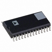
IC ADC STEREO 16BIT 28-SOIC

AD1877JR

Manufacturer Part Number
AD1877JR
Description
IC ADC STEREO 16BIT 28-SOIC
Manufacturer
Analog Devices Inc
Datasheet

Specifications of AD1877JR

Rohs Status
RoHS non-compliant
Number Of Bits
16
Sampling Rate (per Second)
48k
Data Interface
Serial
Number Of Converters
2
Power Dissipation (max)
315mW
Voltage Supply Source
Analog and Digital
Operating Temperature
0°C ~ 70°C
Mounting Type
Surface Mount
Package / Case
28-SOIC (0.300", 7.50mm Width)

Available stocks

Company
Part Number
Manufacturer
Quantity
Price
Part Number:
AD1877JR
Manufacturer:
ADI/亚德诺
Quantity:
20 000
Part Number:
AD1877JRZ
Manufacturer:
ADI/亚德诺
Quantity:
20 000
a
PRODUCT OVERVIEW
The AD1877 is a stereo, 16-bit oversampling ADC based on
Sigma Delta (∑∆) technology intended primarily for digital
audio bandwidth applications requiring a single 5 V power supply.
Each single-ended channel consists of a fourth-order one-bit
noise shaping modulator and a digital decimation filter. An on-
chip voltage reference, stable over temperature and time, defines
the full-scale range for both channels. Digital output data from
both channels are time-multiplexed to a single, flexible serial
interface. The AD1877 accepts a 256 × F
clock (F
port “master” and “slave” modes. In slave mode, all clocks must
be externally derived from a common source.
Input signals are sampled at 64 × F
switched-capacitors, eliminating external sample-and-hold ampli-
fiers and minimizing the requirements for antialias filtering at the
input. With simplified antialiasing, linear phase can be preserved
across the passband. The on-chip single-ended to differential signal
converters save the board designer from having to provide them
externally. The AD1877’s internal differential architecture provides
increased dynamic range and excellent power supply rejection
characteristics. The AD1877’s proprietary fourth-order differen-
tial switched-capacitor ∑∆ modulator architecture shapes the
REV. A
I
Information furnished by Analog Devices is believed to be accurate and
reliable. However, no responsibility is assumed by Analog Devices for its
use, nor for any infringements of patents or other rights of third parties
which may result from its use. No license is granted by implication or
otherwise under any patent or patent rights of Analog Devices.
FEATURES
Single 5 V Power Supply
Single-Ended Dual-Channel Analog Inputs
92 dB (Typ) Dynamic Range
90 dB (Typ) S/(THD+N)
0.006 dB Decimator Passband Ripple
Fourth-Order, 64-Times Oversampling
Three-Stage, Linear-Phase Decimator
256
Less than 100 W (Typ) Power-Down Mode
Input Overrange Indication
On-Chip Voltage Reference
Flexible Serial Output Interface
28-Lead SOIC Package
APPLICATIONS
Consumer Digital Audio Receivers
Digital Audio Recorders, Including Portables
Multimedia and Consumer Electronic Equipment
Sampling Music Synthesizers
Digital Karaoke Systems
CD-R, DCC, MD and DAT
S
is the sampling frequency) and operates in both serial
F
S
or 384
F
S
Input Clock
S
onto internally buffered
S
or a 384 × F
Modulator
S
input
one-bit comparator’s quantization noise out of the audio pass-
band. The high order of the modulator randomizes the modulator
output, reducing idle tones in the AD1877 to very low levels.
Because its modulator is single-bit, AD1877 is inherently
monotonic and has no mechanism for producing differential
linearity errors.
The input section of the AD1877 uses autocalibration to correct
any dc offset voltage present in the circuit, provided that the inputs
are ac coupled. The single-ended dc input voltage can swing
between 0.7 V and 3.8 V typically. The AD1877 antialias input
circuit requires four external 470 pF NPO ceramic chip filter
capacitors, two for each channel. No active electronics are
needed. Decoupling capacitors for the supply and reference pins
are also required.
The dual digital decimation filters are triple-stage, finite impulse
response filters for effectively removing the modulator’s high
frequency quantization noise and reducing the 64 × F
output data rate to an F
and a narrow transition band that properly digitizes 20 kHz signals
at a 44.1 kHz sampling frequency. Passband ripple is less than
0.006 dB, and stopband attenuation exceeds 90 dB.
One Technology Way, P.O. Box 9106, Norwood, MA 02062-9106, U.S.A.
Tel: 781/329-4700
Fax: 781/326-8703
RDEDGE
384/256
DGND1
AGNDL
CAPL1
CAPL2
DV
WCLK
V
LRCK
BCLK
AV
REF
V
DD
S/M
IN
DD
L
L
1
10
12
13
14
11
2
3
4
5
6
9
1
7
8
FUNCTIONAL BLOCK DIAGRAM
THREE-STAGE FIR
DIFFERENTIAL INPUT
DECIMATION
D
A
C
16-Bit
CONVERTER
SINGLE TO
FILTER
World Wide Web Site: http://www.analog.com
SERIAL OUTPUT
S
INTERFACE
word rate. They provide linear phase
REFERENCE
D
A
C
VOLTAGE
DIFFERENTIAL INPUT
THREE-STAGE FIR
D
A
C
Single-Supply
CONVERTER
SINGLE TO
DECIMATION
© Analog Devices, Inc., 2000
FILTER
AD1877
Stereo ADC
AD1877
DIVIDER
CLOCK
D
A
C
(Continued on Page 6)
S
28
27
26
25
24
23
22
21
20
19
18
17
16
15
single-bit
DGND2
CLKIN
TAG
SOUT
DV
RESET
MSBDLY
RLJUST
AGND
V
CAPR2
AGNDR
V
CAPR1
IN
REF
DD
R
R
2

Related parts for AD1877JR

AD1877JR Summary of contents

Page 1

FEATURES Single 5 V Power Supply Single-Ended Dual-Channel Analog Inputs 92 dB (Typ) Dynamic Range 90 dB (Typ) S/(THD+N) 0.006 dB Decimator Passband Ripple Fourth-Order, 64-Times Oversampling Three-Stage, Linear-Phase Decimator 256 F or 384 F Input Clock S S ...

Page 2

AD1877–SPECIFICATIONS TEST CONDITIONS UNLESS OTHERWISE NOTED Supply Voltages Ambient Temperature ) [256 × F Input Clock (F ] CLKIN S Input Signal Measurement Bandwidth Load Capacitance on Digital Outputs Input Voltage Input Voltage ...

Page 3

DIGITAL I/O Input Voltage Input Voltage Input Leakage ( Input Leakage ( Output Voltage ...

Page 4

... AD1877 features proprietary ESD protection circuitry, permanent damage may occur on devices subjected to high-energy electrostatic discharges. Therefore, proper ESD precautions are recommended to avoid performance degradation or loss of functionality. ORDERING GUIDE Package Model Temperature Description AD1877JR 0°C to 70°C SOIC Min 0 –60 Min ...

Page 5

PIN FUNCTION DESCRIPTIONS Input/ Pin Pin Output Name Description 1 I/O LRCK Left/Right Clock 2 I/O WCLK Word Clock 3 I/O BCLK Bit Clock Digital Supply DGND1 Digital Ground 6 I ...

Page 6

AD1877 ( ) Continued from Page 1 The flexible serial output port produces data in twos-comple- ment, MSB-first format. The input and output signals are TTL compatible. The port is configured by pin selections. Each 16-bit output word of a ...

Page 7

Sample Delay The sample delay or “group delay” of the AD1877 is dominated by the processing time of the digital decimation filter. FIR fil- ters convolve a vector representing time samples of the input with an equal-sized vector of coefficients. ...

Page 8

AD1877 The AD1877 also features a power-down mode enabled by the active LO RESET Pin 23 (i.e., the AD1877 is in powerdown mode while RESET is held LO). The power savings are speci- fied in the ‘’Specifications’’ section ...

Page 9

The ground planes should be tied together at one spot under- neath the center of the package with an approximately 3 mm trace. This ground plane technique also minimizes RF transmis- sion and reception. 1 LRCK WCLK 2 BCLK 3 ...

Page 10

AD1877 MSBDLY S/M RLJUST WCLK Output Input Output Output Output Output Output Output Serial Port Data ...

Page 11

Two modes deserve special discussion. The first special mode, “Slave Mode, Data Position Controlled by WCLK Input” (S/M = HI, RLJUST = HI, MSBDLY = LO), shown in Figure 8, is the only mode in which WCLK is an input. ...

Page 12

AD1877–Typical Performance Characteristic Curves 100 120 140 FREQUENCY – kHz TPC 1. 1 kHz Tone at –0.5 dBFS (16k-Point FFT) 0 –20 –40 –60 –80 –100 –120 ...

Page 13

LRCK INPUT BCLK RDEDGE = INPUT BCLK RDEDGE = HI PREVIOUS DATA SOUT ZEROS MSB-14 LSB OUTPUT WCLK OUTPUT LEFT TAG TAG MSB LSB OUTPUT Figure 7. Serial Data Output Timing: Slave Mode, Right-Justified with ...

Page 14

AD1877 LRCK INPUT BCLK RDEDGE = LO INPUT BCLK RDEDGE = HI LEFT DATA SOUT ZEROS MSB OUTPUT MSB-1 WCLK OUTPUT LEFT TAG TAG MSB LSB OUTPUT Figure 9. Serial Data Output Timing: Slave Mode, Left-Justified ...

Page 15

LRCK OUTPUT BCLK RDEDGE = LO OUTPUT BCLK RDEDGE = HI PREVIOUS DATA SOUT MSB-14 LSB OUTPUT WCLK OUTPUT LEFT TAG TAG MSB LSB OUTPUT Figure 12. Serial Data Output Timing. Master Mode, Right-Justified with MSB Delay, ...

Page 16

AD1877 LRCK INPUT BCLK RDEDGE = LO INPUT BCLK RDEDGE = HI PREVIOUS DATA SOUT LSB MSB OUTPUT MSB-14 WCLK OUTPUT TAG MSB OUTPUT Figure 15. Serial Data Output Timing: Slave Mode, Left-Justified with No MSB Delay, ...

Page 17

BCLK INPUT RDEDGE = LO BCLK OUTPUT RDEDGE = HI LRCK INPUT WCLK INPUT DATA & TAG OUTPUTS t CPWH CLKIN INPUT RESET INPUT REV BPWL XMIT SAMPLE XMIT SAMPLE t BPWH t SETLRBS t SETWBS t t ...

Page 18

AD1877 PIN 1 0.0118 (0.30) 0.0040 (0.10) OUTLINE DIMENSIONS Dimensions shown in inches and (mm). R-28 (S-Suffix) 28-Lead Wide-Body SO SOL- 0.2992 (7.60) 0.2914 (7.40) 0.4193 (10.65) 0.3937 (10.00 0.1043 (2.65) 0.7125 (18.10) 0.0926 (2.35) 0.6969 ...

Page 19

–19– ...

Page 20

–20– ...

Related keywords