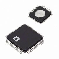
AD6645ASQ-105 Analog Devices Inc, AD6645ASQ-105 Datasheet

AD6645ASQ-105
Specifications of AD6645ASQ-105
Available stocks
Related parts for AD6645ASQ-105
AD6645ASQ-105 Summary of contents
Page 1
FEATURES SNR = 75 dB MHz 105 MSPS IN SNR = 72 dB, f 200 MHz 105 MSPS IN SFDR = 89 dBc MHz 105 MSPS IN 100 dBFS multitone ...
Page 2
AD6645 TABLE OF CONTENTS Features .............................................................................................. 1 Applications ....................................................................................... 1 General Description ......................................................................... 1 Product Highlights ........................................................................... 1 Functional Block Diagram .............................................................. 1 Revision History ............................................................................... 2 Specifications ..................................................................................... 3 DC Specifications ......................................................................... 3 Digital Specifications ................................................................... 4 AC Specifications ...
Page 3
... V ±0 ±1.0 V 2 1.5 II 4.75 5.0 II 3.0 3.3 II 275 1.5 AD8138, Rev Page AD6645ASQ-105/AD6645ASV-105 Max Min Typ Max 14 Guaranteed +10 −10 +1.2 +10 +10 −10 0 +10 +1.5 −1.0 ±0.5 +1.5 ±1.5 1.5 48 ±1.0 2.4 2.2 1 1.5 5.25 4.75 5.0 5.25 3 ...
Page 4
... V 70.0 25°C V 63.5 Rev Page AD6645ASQ-105/AD6645ASV-105 Max Min Typ 0.4 10 2.5 CMOS 2.85 DV − 0.5 0.2 Twos complement 3.3 V; ENCODE, ENCODE , AD6645ASQ-105/ AD6645ASV-105 Max Min Typ Max Unit 75 72.5 74.5 dB 72.0 73.5 dB 73.0 dB 72 72.5 74.5 dB 73 ...
Page 5
... Max Unit 96.0 dBc dBc 86.0 95.0 dBc 90.0 dBc 90.0 dBc 88.0 dBc 98.0 dBFS 98.0 dBFS 98.0 dBFS 90 dBc 270 MHz AD6645ASQ-105/ AD6645ASV-105 Max Min Typ 105 30 4.286 4.75 4.286 4.75 9.5 3.1 1.0 2 ENCH DR 9.4 5.7 6.75 7.0 2 ...
Page 6
... ENCH and t . ENCH ENCH ENCL t ENC E_FL E_DR N – – S_DR t DR Figure 2. Timing Diagram Rev Page AD6645ASQ-105/ AD6645ASV-105 Typ Max Min Typ 5 5 Note 5 Note 5 7.2 7.9 5.1 5 Note 5 Note 5 3.6 5.1 0.6 2.1 −500 −500 0.1 0 E_RL H_E and duty cycle. ...
Page 7
ABSOLUTE MAXIMUM RATINGS Table 5. Parameter Electrical AV Voltage CC DV Voltage CC Analog Input Voltage Analog Input Current Digital Input Voltage Digital Output Current Environmental Operating Temperature Range (Ambient) AD6645-80 AD6645-105 Maximum Junction Temperature Lead Temperature (Soldering, 10 sec) ...
Page 8
AD6645 PIN CONFIGURATION AND FUNCTION DESCRIPTIONS ENCODE ENCODE NOTES 1. DNC = DO NOT CONNECT. 2. EXPOSED PAD. CONNECT THE EXPOSED PAD TO GND. Table 7. Pin Function Descriptions Pin Number Mnemonic 1, 33 10, ...
Page 9
TYPICAL PERFORMANCE CHARACTERISTICS 0 ENCODE = 80MSPS –10 AIN = 2.2MHz @ –1dBFS SNR = 75.0dB –20 SFDR = 93.0dBc –30 –40 –50 –60 –70 –80 3 – –100 6 4 –110 –120 –130 ...
Page 10
AD6645 75.5 75 –40°C 74 +85°C 74 +25°C 73.5 73.0 72.5 ENCODE = 80MSPS @ AIN = –1dBFS TEMP = –40°C, +25°C, +85°C 72 FREQUENCY (MHz) Figure 10. Signal-to-Noise ...
Page 11
ENCODE = 80MSPS –10 AIN = 30.5MHz, 31.5MHz (–7dBFS) –20 NO DITHER –30 –40 –50 –60 –70 –80 –90 –100 –110 –120 –130 FREQUENCY (MHz) Figure 16. Two-Tone SFDR @ 30.5 MHz ...
Page 12
AD6645 0 ENCODE = 80.0MSPS –10 AIN = 30.5MHz @ –29.5dBFS NO DITHER –20 –30 –40 –50 –60 –70 –80 2 –90 6 –100 3 –110 5 –120 –130 FREQUENCY (MHz) Figure 22. 1 ...
Page 13
ENCODE = 76.8MSPS –10 AIN = 2W-CDMA @ 59.6MHz –20 –30 –40 –50 –60 –70 –80 –90 –100 –110 –120 –130 FREQUENCY (MHz) Figure 28. Two W-CDMA Carriers @ 59.6 MHz, Encode = ...
Page 14
AD6645 EQUIVALENT CIRCUITS AIN BUF 500Ω BUF 500Ω AIN BUF V CL Figure 32. Analog Input Stage LOADS 10kΩ ENCODE 10kΩ LOADS Figure 33. Encode Inputs ...
Page 15
TERMINOLOGY Analog Bandwidth The analog input frequency at which the spectral power of the fundamental frequency (as determined by the FFT analysis) is reduced by 3 dB. Aperture Delay The delay between the 50% point of the rising edge of ...
Page 16
AD6645 Spurious-Free Dynamic Range (SFDR) The ratio of the rms signal amplitude to the rms value of the peak spurious spectral component. The peak spurious component may or may not be a harmonic. May be reported in dBc (that is, ...
Page 17
THEORY OF OPERATION The AD6645 ADC employs a three-stage subrange architecture. This design approach achieves the required accuracy and speed while maintaining low power and small die size. As shown in the functional block diagram (see Figure 1), the AD6645 ...
Page 18
AD6645 This limits the amount of dynamic current from the A/D flowing back into the secondary of the transformer. The 50 Ω impedance matching can also be incorporated on the secondary side of the transformer, as shown in the evaluation ...
Page 19
LAYOUT INFORMATION The schematic of the evaluation board (see Figure 43) represents a typical implementation of the AD6645. A multi- layer board is recommended to achieve best results highly recommended that high quality, ceramic chip capacitors be used ...
Page 20
... Samtec TSW-120-08-T-D-RA Johnson Components 142-0701-201 Coilcraft 1008CT-040X-J Panasonic ERJ-2RKF1000 Panasonic ERJ-8ENF60R4V Panasonic ERJ-6ENF4990V Panasonic ERJ-6ENF25R5V Panasonic ERJ-6ENF66R5V Panasonic ERJ-6ENF1000V Panasonic ERJ-2RKF1780X Panasonic ERJ-6ENF49R9V Panasonic EXB2HV101JV Mini-Circuits ADT4-1WT Analog Devices AD6645ASQ/ASV-80 Analog Devices AD6645ASQ/ASV-105 Fairchild 74LCX574WM Analog Devices AD8138AR Fairchild NC7SZ32 ...
Page 21
Quantity Quantity 80 MSPS 105 MSPS Reference (U8 AC-coupled AIN is standard: R3, R4, R5, R8, and U3 are not installed. If dc-coupled AIN is required, ...
Page 22
AD6645 ...
Page 23
Figure 44. Top Signal Level Figure 45. 5.0 V Plane Layer 3 and 3.3 V Plane Layer 4 Figure 46. Ground Plane Layer 2 and Ground Plane Layer 5 Figure 47. Bottom Signal Layer Rev Page 23 of ...
Page 24
... VIEW A ROTATED 90 ° CCW ORDERING GUIDE Model Temperature Range AD6645ASQ-80 −40°C to +85°C 1 AD6645ASQZ-80 −40°C to +85°C 1 AD6645ASVZ-80 −40°C to +85°C AD6645ASQ-105 −10°C to +85°C 1 AD6645ASQZ-105 −10°C to +85°C 1 AD6645ASVZ-105 −10°C to +85°C 1 AD6645-80/PCBZ 1 AD6645-105/PCBZ RoHS Compliant Part. © ...


