AD6645ASQ-105 Analog Devices Inc, AD6645ASQ-105 Datasheet - Page 8
AD6645ASQ-105
Manufacturer Part Number
AD6645ASQ-105
Description
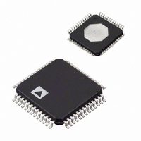
IC ADC 14BIT 105MSPS 52-LQFP-PQ4
Manufacturer
Analog Devices Inc
Datasheet
1.AD6645ASVZ-80.pdf
(24 pages)
Specifications of AD6645ASQ-105
Rohs Status
RoHS non-compliant
Design Resources
Low Jitter Sampling Clock Generator for High Performance ADCs Using AD9958/9858 and AD9515 (CN0109)
Number Of Bits
14
Sampling Rate (per Second)
105M
Data Interface
Parallel
Number Of Converters
4
Power Dissipation (max)
1.75W
Voltage Supply Source
Analog and Digital
Operating Temperature
-10°C ~ 85°C
Mounting Type
Surface Mount
Package / Case
52-LQFP Exposed Pad, 52-eLQFP, 52-HLQFP
For Use With
AD6645-80/PCBZ - BOARD EVAL ADC 80MSPS AD6645AD6645-MIL/PCB - BOARD EVAL AD6645-MIL/PCB
Available stocks
Company
Part Number
Manufacturer
Quantity
Price
Company:

Part Number:
AD6645ASQ-105
Manufacturer:
MAXIM
Quantity:
17 600
Company:
Part Number:
AD6645ASQ-105
Manufacturer:
AD
Quantity:
648
Part Number:
AD6645ASQ-105
Manufacturer:
ADI/亚德诺
Quantity:
20 000


AD6645
PIN CONFIGURATION AND FUNCTION DESCRIPTIONS
Table 7. Pin Function Descriptions
Pin Number
1, 33, 43
2, 4, 7, 10, 13, 15, 17, 19, 21, 23, 25,
27, 29, 34, 42
3
5
6
8, 9, 14, 16, 18, 22, 26, 28, 30
11
12
20
24
31
32
35
36
37 to 41, 44 to 50
51
52
53 (EPAD)
Mnemonic
DV
GND
VREF
ENCODE
ENCODE
AV
AIN
AIN
C1
C2
DNC
OVR
DMID
D0 (LSB)
D1 to D5, D6 to D12
D13 (MSB)
DRY
Exposed Paddle (EPAD)
ENCODE
ENCODE
NOTES
1. DNC = DO NOT CONNECT.
2. EXPOSED PAD. CONNECT THE EXPOSED PAD TO GND.
CC
CC
VREF
DV
AV
AV
GND
GND
GND
GND
GND
AIN
AIN
CC
CC
CC
10
11
12
13
1
2
3
4
5
6
7
8
9
52
14
51
PIN 1
IDENTIFIER
15 16 17 18 19 20 21 22 23 24 25 26
50
Figure 3. Pin Configuration
49
Rev. D | Page 8 of 24
48
(Not to Scale)
AD6645
TOP VIEW
Description
3.3 V Power Supply (Digital) Output Stage Only.
Ground.
2.4 V Reference. Bypass to ground with a 0.1 μF microwave chip capacitor.
Encode Input. Conversion initiated on rising edge.
Complement of ENCODE , Differential Input.
5 V Analog Power Supply.
Analog Input.
Complement of AIN, Differential Analog Input.
Internal Voltage Reference. Bypass to ground with a 0.1 μF chip capacitor.
Internal Voltage Reference. Bypass to ground with a 0.1 μF chip capacitor.
Do not connect this pin.
Overrange Bit. A logic level high indicates analog input exceeds ±FS.
Output Data Voltage Midpoint. Approximately equal to (DV
Digital Output Bit (Least Significant Bit); Twos Complement.
Digital Output Bits in Twos Complement.
Digital Output Bit (Most Significant Bit); Twos Complement.
Data-Ready Output.
Exposed Pad. Connect the exposed pad to GND.
47
46
45
44
43
42
41
40
39
38
37
36
35
34
33
32
31
30
29
28
27
D3
D2
D1
D0 (LSB)
DMID
GND
DV
OVR
DNC
AV
GND
AV
GND
CC
CC
CC
CC
)/2.
Related parts for AD6645ASQ-105
Image
Part Number
Description
Manufacturer
Datasheet
Request
R

Part Number:
Description:
Monolithic 12-Bit Quad DAC
Manufacturer:
Analog Devices
Datasheet:

Part Number:
Description:
±1.7g Dual-Axis IMEMS Accelerometer Evaluation Board
Manufacturer:
Analog Devices Inc
Datasheet:

Part Number:
Description:
Inertial Sensor Evaluation System
Manufacturer:
Analog Devices Inc
Datasheet:
Part Number:
Description:
Manufacturer:
Analog Devices Inc
Datasheet:
Part Number:
Description:
Manufacturer:
Analog Devices Inc
Datasheet:
Part Number:
Description:
Manufacturer:
Analog Devices Inc
Datasheet:
Part Number:
Description:
Manufacturer:
Analog Devices Inc
Datasheet:
Part Number:
Description:
Manufacturer:
Analog Devices Inc
Datasheet:
Part Number:
Description:
Manufacturer:
Analog Devices Inc
Datasheet:
Part Number:
Description:
Manufacturer:
Analog Devices Inc
Datasheet:
Part Number:
Description:
Manufacturer:
Analog Devices Inc
Datasheet:
Part Number:
Description:
Manufacturer:
Analog Devices Inc
Datasheet:
Part Number:
Description:
Manufacturer:
Analog Devices Inc
Datasheet: