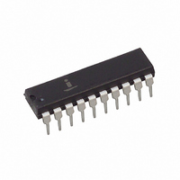
ADC0804LCN Intersil, ADC0804LCN Datasheet - Page 12

ADC0804LCN
Manufacturer Part Number
ADC0804LCN
Description
IC ADC 8-BIT 10KSPS 1LSB 20-DIP
Manufacturer
Intersil
Datasheet
1.ADC0804LCN.pdf
(17 pages)
Specifications of ADC0804LCN
Number Of Bits
8
Sampling Rate (per Second)
10k
Data Interface
Parallel
Number Of Converters
1
Voltage Supply Source
Single Supply
Operating Temperature
0°C ~ 70°C
Mounting Type
Through Hole
Package / Case
20-DIP (0.300", 7.62mm)
Lead Free Status / RoHS Status
Contains lead / RoHS non-compliant
Other names
ADC0804LCNIN
ADC0804LCNIN
ADC0804LCNIN
Available stocks
Company
Part Number
Manufacturer
Quantity
Price
Company:
Part Number:
ADC0804LCN
Manufacturer:
MICROCHIP
Quantity:
2 000
Company:
Part Number:
ADC0804LCN
Manufacturer:
NS
Quantity:
432
Company:
Part Number:
ADC0804LCN
Manufacturer:
TI
Quantity:
100
Part Number:
ADC0804LCN
Manufacturer:
NS/国半
Quantity:
20 000
Company:
Part Number:
ADC0804LCN*
Manufacturer:
S/PHI
Quantity:
19
Company:
Part Number:
ADC0804LCN/NOPB
Manufacturer:
MICRON
Quantity:
1 000
Finally, if time is short and capacitive loading is high, external
bus drivers must be used. These can be three-state buffers
(low power Schottky is recommended, such as the 74LS240
series) or special higher-drive-current products which are
designed as bus drivers. High-current bipolar bus drivers
with PNP inputs are recommended.
Power Supplies
Noise spikes on the V+ supply line can cause conversion
errors as the comparator will respond to this noise. A
low-inductance tantalum filter capacitor should be used
close to the converter V+ pin, and values of 1 F or greater
are recommended. If an unregulated voltage is available in
the system, a separate 5V voltage regulator for the converter
(and other analog circuitry) will greatly reduce digital noise
on the V+ supply. An lCL7663 can be used to regulate such
a supply from an input as low as 5.2V.
Wiring and Hook-Up Precautions
Standard digital wire-wrap sockets are not satisfactory for
breadboarding with this A/D converter. Sockets on PC
boards can be used. All logic signal wires and leads should
be grouped and kept as far away as possible from the
analog signal leads. Exposed leads to the analog inputs can
cause undesired digital noise and hum pickup; therefore,
shielded leads may be necessary in many applications.
A single-point analog ground should be used which is
separate from the logic ground points. The power supply
bypass capacitor and the self-clockIng capacitor (if used)
should both be returned to digital ground. Any V
bypass capacitors, analog input filter capacitors, or input
signal shielding should be returned to the analog ground
point. A test for proper grounding is to measure the zero
error of the A/D converter. Zero errors in excess of
can usually be traced to improper board layout and wiring
(see Zero Error for measurement). Further information can
be found in Application Note AN018.
Testing the A/D Converter
There are many degrees of complexity associated with testing
an A/D converter. One of the simplest tests is to apply a
known analog input voltage to the converter and use LEDs to
display the resulting digital output code as shown in Figure 18.
For ease of testing, the V
with 2.560V and a V+ supply voltage of 5.12V should be
used. This provides an LSB value of 20mV.
If a full scale adjustment is to be made, an analog input
voltage of 5.090V (5.120 - 1
the V
V
output code is just changing from 1111 1110 to 1111 1111.
This value of V
The digital-output LED display can be decoded by dividing
the 8 bits into 2 hex characters, one with the 4 most-
REF
IN(+)
/2 input voltage should be adjusted until the digital
pin with the V
REF
/2 should then be used for all the tests.
IN(-)
REF
1
12
pin grounded. The value of the
/2 (pin 9) should be supplied
/
2
LSB) should be applied to
REF
ADC0803, ADC0804
1
/2
/
4
LSB
significant bits (MS) and one with the 4 least-significant bits
(LS). The output is then interpreted as a sum of fractions
times the full scale voltage:
For example, for an output LED display of 1011 0110, the
MS character is hex B (decimal 11) and the LS character is
hex (and decimal) 6, so:
V OUT
Figures 19 and 20 show more sophisticated test circuits.
Typical Applications
Interfacing 8080/85 or Z-80 Microprocessors
V
START
V
2.560V
ANALOG
V
OUT
FIGURE 19. A/D TESTER WITH ANALOG ERROR OUTPUT. THIS
REF
INPUTS
IN
150pF
(+)
/2
DIGITAL
INPUTS
=
=
AGND
0.1 F
0.1 F
N.O.
FIGURE 20. BASIC “DIGITAL” A/D TESTER
MS
-------- -
11
----- -
16
FIGURE 18. BASIC TESTER FOR THE A/D
16
+
+
CIRCUIT CAN BE USED TO GENERATE “ERROR
PLOTS” OF FIGURE 11.
“A”
--------- -
256
--------- -
256
LS
6
10-BIT
DAC
A/D UNDER
5.12
5.12 V
R
TEST
8-BIT
R
“B”
10
DGND
1
2
3
4
5
6
7
8
9
10k
V
=
ANALOG
ADC0803-
ADC0804
.
3.64V
A1
100R
R
+
-
.
A/D UNDER
+
-
A2
10-BIT
TEST
DAC
20
19
18
17
16
15
14
13
12
11
1.3k
R
(8)
100X ANALOG
ERROR VOLTAGE
V
ANALOG OUTPUT
OUTPUTS
+
DIGITAL
“C”
10 F
TANTALUM
LEDs
(8)
5.120V
LSB
MSB
5V


