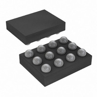
MAX11803EWC+T Maxim Integrated Products, MAX11803EWC+T Datasheet - Page 39

MAX11803EWC+T
Manufacturer Part Number
MAX11803EWC+T
Description
IC TOUCH SCREEN CTLR 12-WLP
Manufacturer
Maxim Integrated Products
Type
Resistiver
Datasheet
1.MAX11803EWCT.pdf
(59 pages)
Specifications of MAX11803EWC+T
Touch Panel Interface
4-Wire
Number Of Inputs/keys
1 TSC
Resolution (bits)
12 b
Data Interface
I²C, Serial
Data Rate/sampling Rate (sps, Bps)
105k
Voltage - Supply
1.7 V ~ 3.6 V
Operating Temperature
-40°C ~ 85°C
Mounting Type
Surface Mount
Package / Case
12-WLP
Voltage Supply Source
Single Supply
Sampling Rate (per Second)
105k
Resolution
11 bits
Interface Type
I2C, SPI
Supply Voltage (max)
3.6 V
Supply Voltage (min)
1.7 V
Conversion Rate
34.4 KSPs
Maximum Operating Temperature
+ 85 C
Minimum Operating Temperature
- 40 C
Mounting Style
SMD/SMT
Lead Free Status / RoHS Status
Lead free / RoHS Compliant
Other names
MAX11803EWC+T
MAX11803EWC+TTR
MAX11803EWC+TTR
Figure 19 shows the read operation sequence for the
MAX11800/MAX11802. A single configuration register
can be read back in a 2-byte operation, composed of a
requested register address (A[6:0], plus a read mode
indicator bit) followed by the data contents from that reg-
ister (D[7:0]).
During read operations, the SPI takes control of the DOUT
line following the eight SCLK rising edge. The SPI retains
control of the DOUT line until CS rises, terminating the
operation. To support multiple register readback opera-
tions, data continues to be ported following the 16th rising
clock edge. For single-byte transfers, this sub-bit informa-
tion can be ignored, shown as S, in Figure 19.
The DOUT output on the MAX11800/MAX11802 includes
an optional bus holder to prevent the DOUT line from
maintaining an indeterminate state when vacated by the
device in the absence of an external bus pullup or bus
sharing devices. The bus holder is designed not to inter-
fere with other drivers sharing the DOUT line and holds
the last valid state of the line, regardless of source.
Disable the bus holder when not needed.
The MAX11800/MAX11802 support the combination of
the DIN and DOUT lines. To avoid data contention and
possible high current states, the master device must relin-
quish control of the combined line at the 8th clock rising
edge, allowing the MAX11800/MAX11802 to access the
line through the end of the sequence. This is terminated
on the rising edge of CS. See the SPI Timing
Characteristics for relevant details.
The MAX11800/MAX11802 also support multiple register
readback operations using a single command. The proto-
col requires the user to supply an initial starting register
location, followed by an unlimited number of clock pulses
for data readback.
The first data read back is from the start register. The
MAX11800/MAX11802 internal autoincrement counter
manages the data readback in later cycles. If autoin-
Figure 19. SPI Single-Byte Register Read Sequence—MAX11800/MAX11802
Low-Power, Ultra-Small Resistive Touch-Screen
Result Register Read (MAX11800/MAX11802)
DOUT
SCLK
DIN
CS
______________________________________________________________________________________
A6
1
A5
2
A4
3
SPI Configuration or
Controllers with I
A3
4
A2
5
A1
6
A0
7
R
8
D7
crement is supported, the next register location is read
back. If not, the last valid register location is read back
(see the Command and Register Map section for the
autoincrement attributes of each register). The following
example shows a valid sequence for the readback of
three register locations (D
The autoincrement reads only the X, Y, Z1, Z2, and AUX
result registers preventing inadvertent readback of unre-
lated or reserved data locations. For example, if begin-
ning at the XMSB register, a user can cycle through the
XLSB register to the YMSB register and so forth up to the
AUXLSB register. The MAX11800/MAX11802 do not
autoincrement beyond the AUXLSB register. If clock
cycles continue to be given, the AUXLSB register read-
back is repeated.
The FIFO register does not autoincrement, which allows
multiple readbacks of the same location. This allows the
access of multiple FIFO memory blocks with a single read
operation. When reading back FIFO registers, data man-
agement is handled in blocks not bytes. As a result, when
an SPI read operation supplies at least one cycle of read-
back of the first byte of a FIFO block, the entire block is
marked as read, regardless of whether the block or even
byte readback is run to completion.
To illustrate, assume the MAX11800 is in autonomous
mode performing XY conversions and a FIFO readback
is requested starting at register 0x50. Clock cycles 9 to
40 are required to complete the readback of the first
available FIFO block
with the device updating in response to the 8th to 39th
clock rising edges. The host processor can complete
the readback data latching of YLSB
39th falling edge or the 40th rising edge. To support a
continued readback of further FIFO blocks, the device
updates the DOUT line to XMSB
40th clock rising edge (though block
as read). If the AP supplies a 42nd clock rising edge,
the FIFO block
less of whether any further clock cycles are provided.
9
D6
10
D5
11
D4
i+1
2
12
, if present, is marked as read, regard-
D3
C/SPI Interface
i
13
= {XMSB
D2
i
14
through D
D1
15
i
i+1
, XLSB
D0
[7] in response to the
16
i+2
i+1
i
[0] either on the
S
i
).
, YMSB
is not marked
i
, YLSB
39
i
}


