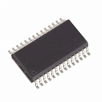
MAX197ACWI+ Maxim Integrated Products, MAX197ACWI+ Datasheet

MAX197ACWI+
Specifications of MAX197ACWI+
Related parts for MAX197ACWI+
MAX197ACWI+ Summary of contents
Page 1
... Data-Acquisition Systems Automatic Testing Systems Medical Instruments Telecommunications Functional Diagram appears at end of data sheet. ________________________________________________________________ Maxim Integrated Products For pricing, delivery, and ordering information, please contact Maxim/Dallas Direct! at 1-888-629-4642, or visit Maxim’s website at www.maxim-ic.com. ____________________________Features o 12-Bit Resolution, 1/2LSB Linearity o Single +5V Operation o Software-Selectable Input Ranges: ± ...
Page 2
Multi-Range (±10V, ±5V, +10V, +5V), Single +5V, 12-Bit DAS with 8+4 Bus Interface ABSOLUTE MAXIMUM RATINGS V to AGND............................................................-0.3V to +7V DD AGND to DGND.....................................................-0.3V to +0.3V REF to AGND..............................................-0. REFADJ to AGND.......................................-0. Digital Inputs to ...
Page 3
Multi-Range (±10V, ±5V, +10V, +5V), Single +5V, 12-Bit DAS with 8+4 Bus Interface ELECTRICAL CHARACTERISTICS (continued ±5%; unipolar/bipolar range; external reference mode with 50% duty cycle MIN MAX PARAMETER ...
Page 4
Multi-Range (±10V, ±5V, +10V, +5V), Single +5V, 12-Bit DAS with 8+4 Bus Interface ELECTRICAL CHARACTERISTICS (continued ±5%; unipolar/bipolar range; external reference mode with 50% duty cycle unless otherwise noted.) ...
Page 5
Multi-Range (±10V, ±5V, +10V, +5V), Single +5V, 12-Bit DAS with 8+4 Bus Interface TIMING CHARACTERISTICS ( ±5%; unipolar/bipolar range; external reference mode with 50% duty cycle MIN MAX PARAMETER SYMBOL ...
Page 6
Multi-Range (±10V, ±5V, +10V, +5V), Single +5V, 12-Bit DAS with 8+4 Bus Interface __________________________________________Typical Operating Characteristics (T = +25°C, unless otherwise noted.) A INTEGRAL NONLINEARITY vs. DIGITAL CODE 0.250 0.200 0.150 0.100 0.050 0.000 -0.050 -0.100 -0.150 0 1000 2000 ...
Page 7
Multi-Range (±10V, ±5V, +10V, +5V), Single +5V, 12-Bit DAS with 8+4 Bus Interface ______________________________________________________________Pin Description PIN NAME Clock Input. In external clock mode, drive CLK with a TTL/CMOS compatible clock. In internal clock mode, 1 CLK place a capacitor from ...
Page 8
Multi-Range (±10V, ±5V, +10V, +5V), Single +5V, 12-Bit DAS with 8+4 Bus Interface _______________Detailed Description Converter Operation The MAX197, a multi-range, fault-tolerant ADC, uses successive approximation and internal input track/hold (T/H) circuitry to convert an analog signal to a 12-bit ...
Page 9
Multi-Range (±10V, ±5V, +10V, +5V), Single +5V, 12-Bit DAS with 8+4 Bus Interface The input channels are overvoltage protected to ±16.5V. This protection is active even if the device is in power-down mode. Even with V = 0V, the input ...
Page 10
Multi-Range (±10V, ±5V, +10V, +5V), Single +5V, 12-Bit DAS with 8+4 Bus Interface Table 6. Data-Bus Output PIN HBEN = LOW HBEN = HIGH D0 B0 (LSB B10 D3 B3 B11 (MSB ...
Page 11
Multi-Range (±10V, ±5V, +10V, +5V), Single +5V, 12-Bit DAS with 8+4 Bus Interface CSWS CONTROL D7–D0 BYTE ACQMOD = "1" INT RD HBEN DOUT Figure 6. Conversion Timing Using External Acquisition ...
Page 12
Multi-Range (±10V, ±5V, +10V, +5V), Single +5V, 12-Bit DAS with 8+4 Bus Interface External Clock Mode Select external clock mode by writing the control byte with and Figure 8 shows CLK and WR timing ...
Page 13
Multi-Range (±10V, ±5V, +10V, +5V), Single +5V, 12-Bit DAS with 8+4 Bus Interface __________Applications Information At power-up, the internal power-supply circuitry sets INT high and puts the device in normal operation/external clock mode. This state is selected to keep the ...
Page 14
Multi-Range (±10V, ±5V, +10V, +5V), Single +5V, 12-Bit DAS with 8+4 Bus Interface Power-Down Mode To save power, you can put the converter into low- current shutdown mode between conversions. Two programmable power-down modes are available, in addition to a ...
Page 15
Multi-Range (±10V, ±5V, +10V, +5V), Single +5V, 12-Bit DAS with 8+4 Bus Interface Transfer Function Output data coding for the MAX197 is binary in unipo- lar mode with 1LSB = (FS / 4096) and two’s-comple- ment binary in bipolar mode ...
Page 16
... Maxim cannot assume responsibility for use of any circuitry other than circuitry entirely embodied in a Maxim product. No circuit patent licenses are implied. Maxim reserves the right to change the circuitry and specifications without notice at any time. 16 __________________Maxim Integrated Products, 120 San Gabriel Drive, Sunnyvale, CA 94086 (408) 737-7600 © 2001 Maxim Integrated Products ...


