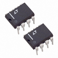
LTC1287CCN8 Linear Technology, LTC1287CCN8 Datasheet

LTC1287CCN8
Specifications of LTC1287CCN8
Available stocks
Related parts for LTC1287CCN8
LTC1287CCN8 Summary of contents
Page 1
... Given the ease of use, small package size and the minimum number of interconnects for I/O, the LTC1287 can be used for remote sensing applications. , LTC and LT are registered trademarks of Linear Technology Corporation. LTCMOS is a trademark of Linear Technology Corporation 22 F TANTALUM + ...
Page 2
... See Test Circuits See Test Circuits See Test Circuits U W ORDER PART TOP VIEW NUMBER CLK LTC1287BCN8 6 D LTC1287CCN8 OUT 5 V REF N8 PACKAGE = 130 C/W ( PACKAGE LTC1287BCJ8 LTC1287CCJ8 = 100 C/W (J) JA OBSOLETE PACKAGE Consider N8 Package for Alternate Source The denotes the specifications = 25 C ...
Page 3
AC CHARACTERISTICS otherwise specifications are (Note 3) A SYMBOL PARAMETER t Time Output Data Remains Valid After CLK hDO t D Fall Time f OUT t D Rise Time r OUT t CLK High Time ...
Page 4
LTC1287 W U TYPICAL PERFOR A Supply Current vs Supply Voltage 2.8 CLK = 500kHz 2 2.4 2.2 2.0 1.8 1.6 1.4 1.2 1.0 0.8 2.7 2.8 2.9 3.0 3.1 3.2 3.3 3.4 3.5 3.6 ...
Page 5
W U TYPICAL PERFOR A Maximum Clock Rate vs Source Resistance 500 2.5V REF CLK = 500kHz 400 300 200 +V +IN IN 100 R – SOURCE –IN 0 100 1k 10k 100k R ...
Page 6
LTC1287 W BLOCK I D AGRA INPUT SHIFT REGISTER 2 +IN ANALOG 3 INPUT MUX –IN 4 GND TEST CIRCUITS On and Off Channel Leakage Current OFF A POLARITY Load Circuit for ...
Page 7
TEST CIRCUITS CS CLK D OUT PPLICATI S I FOR ATIO The LTC1287 is a data acquisition component which contains the following functional blocks: 1. 12-bit successive approximation capacitive A/D converter 2. Analog multiplexer (MUX) 3. ...
Page 8
LTC1287 PPLICATI S I FOR ATIO specified at 3.3V. The output D is also compatible with OUT the above standards. The following summarizes such levels. V (no load) V – 0. (no load) ...
Page 9
PPLICATI S I FOR ATIO such as obtained from a voltage regulator (e.g., LT1117). For high frequency bypassing a 0.1 F ceramic disk placed in parallel with the recommended. Again the leads should ...
Page 10
LTC1287 PPLICATI S I FOR ATIO “+” Input Settling The input capacitor is switched onto the “+” input during the sample phase (t , see Figures 8a, 8b and 8c). The SMPL sample period can be ...
Page 11
PPLICATI S I FOR ATIO CS CLK D OUT (+) INPUT (–) INPUT effectively “held” by the sample and hold and will not affect the conversion result critical that the “–” input voltage be ...
Page 12
LTC1287 PPLICATI S I FOR ATIO RC Input filtering It is possible to filter the inputs with an RC network as shown in Figure 11. For large values of C capacitive input switching currents are averaged ...
Page 13
PPLICATI S I FOR ATIO conversion (every CLK cycle) a capacitive current spike will be generated on the reference pin by the A/D. These current spikes settle quickly and do not cause a prob- lem. If ...
Page 14
LTC1287 PPLICATI S I FOR ATIO curve of Noise Error vs Reference Voltage shows the LSB contribution of this 200 V of noise. For operation with a 2.5V reference, the 200 V noise is only 0.32LSB ...
Page 15
... Figure 20. Scope Trace of the LTC1287 “Quick Look” Circuit Showing A/D Output 1010101010 (AAA Information furnished by Linear Technology Corporation is believed to be accurate and reliable. However, no responsibility is assumed for its use. Linear Technology Corporation makes no representation that the interconnection of circuits as described herein will not infringe on existing patent rights “ ...
Page 16
... MAX (0.127) MIN 0.025 0.220 – 0.310 (0.635) (5.588 – 7.874) RAD TYP 0.125 3.175 MIN 0.400* (10.160) MAX 0.255 0.015* (6.477 0.381 1098 LT/TP 0102 1.5K REV A • PRINTED IN USA LINEAR TECHNOLOGY CORPORATION 1992 0.200 (5.080) MAX J8 1298 1287fa ...


