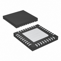
MAX1020BETX+ Maxim Integrated Products, MAX1020BETX+ Datasheet - Page 24

MAX1020BETX+
Manufacturer Part Number
MAX1020BETX+
Description
IC ADC/DAC 10BIT 36-TQFN-EP
Manufacturer
Maxim Integrated Products
Type
ADC, DACr
Datasheet
1.MAX1020BETX.pdf
(44 pages)
Specifications of MAX1020BETX+
Resolution (bits)
10 b
Sampling Rate (per Second)
225k
Data Interface
MICROWIRE™, QSPI™, Serial, SPI™
Voltage Supply Source
Analog and Digital
Voltage - Supply
4.75 V ~ 5.25 V
Operating Temperature
-40°C ~ 85°C
Mounting Type
Surface Mount
Package / Case
36-TQFN Exposed Pad
Lead Free Status / RoHS Status
Lead free / RoHS Compliant
10-Bit, Multichannel ADCs/DACs with FIFO,
Temperature Sensing, and GPIO Ports
Select active analog input channels, scan modes, and
a single temperature measurement per scan by issuing
a command byte to the conversion register. Table 4
details channel selection, the four scan modes, and
how to request a temperature measurement. Start a
scan by writing to the conversion register when in clock
mode 10 or 11, or by applying a low pulse to the
CNVST pin when in clock mode 00 or 01. See Figures 6
and 7 for timing specifications for starting a scan with
CNVST.
A conversion is not performed if it is requested on a
channel or one of the channel pairs that has been con-
figured as CNVST or REF2. For channels configured as
differential pairs, the CHSEL0 bit is ignored and the two
pins are treated as a single differential channel.
Select scan mode 00 or 01 to return one result per sin-
gle-ended channel and one result per differential pair
within the selected scanning range (set by bits 2 and 1,
SCAN1 and SCAN0), plus one temperature result if
selected. Select scan mode 10 to scan a single input
channel numerous times, depending on NSCAN1 and
NSCAN0 in the ADC averaging register (Table 9).
Select scan mode 11 to return only one result from a
single channel.
Issue a command byte to the setup register to config-
ure the clock, reference, power-down modes, and ADC
single-ended/differential modes. Table 5 details the bits
in the setup-register command byte. Bits 5 and 4
(CKSEL1 and CKSEL0) control the clock mode, acqui-
sition and sampling, and the conversion start. Bits 3
and 2 (REFSEL1 and REFSEL0) set the device for either
internal or external reference. Bits 1 and 0 (DIFFSEL1
and DIFFSEL0) address the ADC unipolar-mode and
bipolar-mode registers and configure the analog-input
channels for differential operation.
The ADC reference is always on if any of the following
conditions are true:
1)The FBGON bit is set to one in the reset register.
2)At least one DAC output is powered up and
3)At least one DAC is powered down through the
24
REFSEL[1:0] (in the setup register) = 00.
100kΩ to V
______________________________________________________________________________________
REF
and REFSEL[1:0] = 00.
Conversion Register
Setup Register
Table 4. Conversion Register*
* See below for bit details.
SCAN1
CHSEL3
CHSEL2
CHSEL1
CHSEL0
CHSEL3
SCAN1
SCAN0
NAME
TEMP
0
0
1
1
BIT
—
0
0
0
0
0
0
0
0
1
1
1
1
1
1
1
1
SCAN0
7 (MSB)
0 (LSB)
CHSEL2
0
1
0
1
BIT
6
5
4
3
2
1
0
0
0
0
1
1
1
1
0
0
0
0
1
1
1
1
Scans channels 0 through N.
Scans channels N through the highest
numbered channel.
S cans channel N r epeated l y. The AD C
aver ag ing reg i ster sets the numb er of
r esul ts.
N o scan. C onver ts channel N once onl y.
S et to one to sel ect conver si on r eg i ster .
Analog-input channel select.
Analog-input channel select.
Analog-input channel select.
Analog-input channel select.
Scan-mode select.
Scan-mode select.
Set to one to take a single temp-
erature measurement. The first
conversion result of a scan contains
temperature information.
(CHANNEL N IS SELECTED BY
CHSEL1
BITS CHSEL3–CHSEL0)
0
0
1
1
0
0
1
1
0
0
1
1
0
0
1
1
SCAN MODE
FUNCTION
CHSEL0
0
1
0
1
0
1
0
1
0
1
0
1
0
1
0
1
SELEC T ED
C H AN N EL
AIN10
AIN11
AIN12
AIN13
AIN14
AIN15
AIN0
AIN1
AIN2
AIN3
AIN4
AIN5
AIN6
AIN7
AIN8
AIN9
( N )


