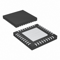
MAX1020BETX+ Maxim Integrated Products, MAX1020BETX+ Datasheet - Page 34

MAX1020BETX+
Manufacturer Part Number
MAX1020BETX+
Description
IC ADC/DAC 10BIT 36-TQFN-EP
Manufacturer
Maxim Integrated Products
Type
ADC, DACr
Datasheet
1.MAX1020BETX.pdf
(44 pages)
Specifications of MAX1020BETX+
Resolution (bits)
10 b
Sampling Rate (per Second)
225k
Data Interface
MICROWIRE™, QSPI™, Serial, SPI™
Voltage Supply Source
Analog and Digital
Voltage - Supply
4.75 V ~ 5.25 V
Operating Temperature
-40°C ~ 85°C
Mounting Type
Surface Mount
Package / Case
36-TQFN Exposed Pad
Lead Free Status / RoHS Status
Lead free / RoHS Compliant
10-Bit, Multichannel ADCs/DACs with FIFO,
Temperature Sensing, and GPIO Ports
If the first byte of an entry in the FIFO is partially read
(CS is pulled high after fewer than eight SCLK cycles),
the remaining bits are lost for that byte. The next byte of
data that is read out contains the next 8 bits. If the first
byte of an entry in the FIFO is read out fully, but the
second byte is read out partially, the rest of that byte is
lost. The remaining data in the FIFO is unaffected and
can be read out normally after taking CS low again, as
long as the 4 leading bits (normally zeros) are ignored.
If CS is pulled low before EOC goes low, a conversion
may not be completed and the FIFO data may not be
correct. Incorrect writes (pulling CS high before com-
pleting eight SCLK cycles) are ignored and the register
remains unchanged.
In clock mode 00, the wake-up, acquisition, conversion,
and shutdown sequence is initiated through CNVST
and performed automatically using the internal oscilla-
tor. Results are added to the internal FIFO to be read
out later. See Figure 6 for clock mode 00 timing after a
command byte is issued. See Table 5 for details on
programming the clock mode in the setup register.
Initiate a scan by setting CNVST low for at least 40ns
before pulling it high again. The MAX1020/MAX1022/
Figure 3. Unipolar Transfer Function—Full Scale (FS) = V
34
______________________________________________________________________________________
111....111
111....110
111....101
000....011
000....010
000....001
000....000
Internally Timed Acquisitions and
Partial Reads and Partial Writes
Applications Information
0
ADC Conversions in Clock Mode 00
FS = V
1 LSB = V
1
2
REF
Conversions Using CNVST
3
REF
INPUT VOLTAGE (LSB)
/ 1024
FULL-SCALE
TRANSITION
FS - 3/2 LSB
FS
REF
MAX1057/MAX1058 then wake up, scan all requested
channels, store the results in the FIFO, and shut down.
After the scan is complete, EOC is pulled low and the
results are available in the FIFO. Wait until EOC goes
low before pulling CS low to communicate with the seri-
al interface. EOC stays low until CS or CNVST is pulled
low again. A temperature-conversion result, if request-
ed, precedes all other FIFO results. Temperature
results are available in 12-bit format.
Figure 4. Bipolar Transfer Function—Full Scale ( ± FS) = ± V REF / 2
Figure 5. Temperature Transfer Function
011....111
011....110
000....010
000....001
000....000
111....111
111....110
111....101
100....001
100....000
011....111
011....110
011....101
000....001
000....000
111....111
100....011
100....010
100....001
100....000
OUTPUT CODE
-256
-FS
FS = V
ZS = COM
-FS = -V
1 LSB = V
REF
REF
V
REF
/ 2 + V
REF
INPUT VOLTAGE (LSB)
/ 2
/ 1024
TEMPERATURE (°C)
COM
-1
(COM)
0
0
V
REF
+1
= V
REF+
V
REF
- V
+FS - 1 LSB
REF-
+255.5
V
V
REF
REF
(COM)


