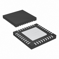
MAX1020BETX+ Maxim Integrated Products, MAX1020BETX+ Datasheet - Page 41

MAX1020BETX+
Manufacturer Part Number
MAX1020BETX+
Description
IC ADC/DAC 10BIT 36-TQFN-EP
Manufacturer
Maxim Integrated Products
Type
ADC, DACr
Datasheet
1.MAX1020BETX.pdf
(44 pages)
Specifications of MAX1020BETX+
Resolution (bits)
10 b
Sampling Rate (per Second)
225k
Data Interface
MICROWIRE™, QSPI™, Serial, SPI™
Voltage Supply Source
Analog and Digital
Voltage - Supply
4.75 V ~ 5.25 V
Operating Temperature
-40°C ~ 85°C
Mounting Type
Surface Mount
Package / Case
36-TQFN Exposed Pad
Lead Free Status / RoHS Status
Lead free / RoHS Compliant
For an ideal converter, the first transition occurs at 0.5
LSB, above zero. Offset error is the amount of deviation
between the measured first transition point and the
ideal first transition point.
While in bipolar mode, the ADC’s ideal midscale transi-
tion occurs at AGND -0.5 LSB. Bipolar offset error is the
measured deviation from this ideal value.
Gain error is defined as the amount of deviation
between the ideal transfer function and the measured
transfer function, with the offset error removed and with
a full-scale analog input voltage applied to the ADC,
resulting in all ones at DOUT.
DAC offset error is determined by loading a code of all
zeros into the DAC and measuring the analog output
voltage.
DAC gain error is defined as the amount of deviation
between the ideal transfer function and the measured
transfer function, with the offset error removed, when
loading a code of all ones into the DAC.
Aperture jitter (t
the time between the samples.
Aperture delay (t
edge of the sampling clock and the instant when an
actual sample is taken.
For a waveform perfectly reconstructed from digital sam-
ples, signal-to-noise ratio (SNR) is the ratio of full-scale
analog input (RMS value) to the RMS quantization error
(residual error). The ideal, theoretical minimum analog-
to-digital noise is caused by quantization error only and
results directly from the ADC’s resolution (N bits):
In reality, there are other noise sources besides quanti-
zation noise, including thermal noise, reference noise,
clock jitter, etc. Therefore, SNR is calculated by taking
the ratio of the RMS signal to the RMS noise. RMS noise
includes all spectral components to the Nyquist fre-
quency excluding the fundamental, the first five har-
monics, and the DC offset.
10-Bit, Multichannel ADCs/DACs with FIFO,
SNR = (6.02 x N + 1.76)dB
AJ
) is the sample-to-sample variation in
______________________________________________________________________________________
AD
) is the time between the rising
Unipolar ADC Offset Error
Bipolar ADC Offset Error
Temperature Sensing, and GPIO Ports
Signal-to-Noise Ratio
DAC Offset Error
ADC Gain Error
DAC Gain Error
Aperture Delay
Aperture Jitter
Signal-to-noise plus distortion (SINAD) is the ratio of the
fundamental input frequency’s RMS amplitude to the
RMS equivalent of all other ADC output signals:
Effective number of bits (ENOB) indicates the global
accuracy of an ADC at a specific input frequency and
sampling rate. An ideal ADC’s error consists of quanti-
zation noise only. With an input range equal to the full-
scale range of the ADC, calculate the ENOB as follows:
Total harmonic distortion (THD) is the ratio of the RMS
sum of the first five harmonics of the input signal to the
fundamental itself. This is expressed as:
where V
V
Spurious-free dynamic range (SFDR) is the ratio of RMS
amplitude of the fundamental (maximum signal compo-
nent) to the RMS value of the next largest distortion
component.
Bias the ON channel to midscale. Apply a full-scale sine
wave test tone to all OFF channels. Perform an FFT on
the ON channel. ADC channel-to-channel crosstalk is
expressed in dB as the amplitude of the FFT spur at the
frequency associated with the OFF channel test tone.
IMD is the total power of the intermodulation products
relative to the total input power when two tones, f1 and
f2, are present at the inputs. The intermodulation prod-
ucts are (f1 ± f2), (2 x f1), (2 x f2), (2 x f1 ± f2), (2 x f2 ±
f1). The individual input tone levels are at -7dBFS.
A small -20dBFS analog input signal is applied to an
ADC so the signal’s slew rate does not limit the ADC’s
performance. The input frequency is then swept up to
the point where the amplitude of the digitized conver-
sion result has decreased by -3dB. Note that the T/H
performance is usually the limiting factor for the small-
signal input bandwidth.
THD
6
are the amplitudes of the first five harmonics.
SINAD(dB) = 20 x log (Signal
=
1
20
is the fundamental amplitude, and V
ADC Channel-to-Channel Crosstalk
x
ENOB = (SINAD - 1.76) / 6.02
Intermodulation Distortion (IMD)
log
Signal-to-Noise Plus Distortion
Spurious-Free Dynamic Range
⎡
⎣ ⎢
(
V
2
Total Harmonic Distortion
2
Effective Number of Bits
+
Small-Signal Bandwidth
V
3
2
+
V
RMS
4
2
+
/ Noise
V
5
2
+
V
RMS
2
6
through
2
)
)
/
V
1
41
⎤
⎦ ⎥


