ADC0858BIV National Semiconductor, ADC0858BIV Datasheet
ADC0858BIV
Specifications of ADC0858BIV


Related parts for ADC0858BIV

ADC0858BIV Summary of contents
Page 1
... Applications Instrumentation monitoring and process control Y Digitizing automotive sensor signals Y Embedded diagnostics Y Simplified Block Diagram TRI-STATE is a registered trademark of National Semiconductor Corporation MICROWIRE trademark of National Semiconductor Corporation C 1995 National Semiconductor Corporation TL H 11021 Key Specifications Resolution Y Total error ...
Page 2
... ADC0851BIN N16E 16-Pin ADC0851CIN Plastic DIP ADC0858BIN N20A 20-Pin ADC0858CIN Plastic DIP ADC0851BIV V20A 20-Lead ADC0851CIV PLCC ADC0858BIV V20A 20-Lead ADC0858CIV PLCC 8-Channel MUX Dual-In-Line Package TL H 11021–1 ADC0858 PLCC Package TL H 11021–3 Military ( 125 ADC0851CMJ 883 ADC0858CMJ 883 ...
Page 3
... J Parameter CONVERTER AND MULTIPLEXER CHARACTERISTICS Total Unadjusted Error (Note 7) ADC0851 8 BIN ADC0851 8 BIV ADC0851 8 CIN ADC0851 8 CMJ ADC0851 8 CIV Comparator Offset ADC0851 8 BIN ADC0858BIV ADC0851 8 CIN ADC0851 8 CMJ ADC0858CIV V Input Resistance REF Common Mode Input Voltage (Note 8) DC Common Mode Error ...
Page 4
DC Electrical Characteristics The following specifications apply for 170 pF) unless otherwise specified Boldface limits apply for T e ext Parameter DIGITAL CHARACTERISTICS Logic ...
Page 5
AC Electrical Characteristics The following specifications apply for unless otherwise specified Boldface limits apply for T Symbol Parameter t t Rising Edge Data Output Hi-Z f Oscillator Clock Freq ...
Page 6
Typical Performance Characteristics Offset Error vs Reference Voltage OSC Frequency vs Temperature Linearity Error vs Total Unadjusted Error Reference Voltage vs Temperature OSC Frequency vs R and C ext ext 11021 – 5 ...
Page 7
Test Circuits and Waveforms Timing Diagrams Data Input Timing 11021 – 11021 – 7 Data Output Timing TL H 11021 – ...
Page 8
Timing Diagrams (Continued) Timing Diagrams for ADC0851 and ADC0858 Read Power Flag after Power Up ADC0851 ADC0858 Watchdog Timing A D Conversion Timing 11021 – 11021 – 11021 – 14 ...
Page 9
Timing Diagrams for ADC0851 and ADC0858 (Continued) 9 ...
Page 10
Timing Diagrams for ADC0851 and ADC0858 (Continued) 10 ...
Page 11
Timing Diagrams for ADC0851 and ADC0858 (Continued) 11 ...
Page 12
ADC0851 Programming Chart Receive (DI) Function Mode Watchdog 1000 C11 C0 Write 1 Limit 1001 Conversion 1010 I3 I0 Read 1 Limit 1011 A3 A0 Test 1100 Write all Limits 1101 4 Bytes L0 ...
Page 13
Pin Descriptions V Positive power supply pin Bypass to analog CC ground with ceramic capacitor in parallel with tantalum capacitor OSC Input Output pin used to generate internal timing for A D conversion ...
Page 14
General Overview The ADC0851 versatile microprocessor-compatible data acquisition system with an on-board watchdog capabili- ty The device is capable of synchronous serial interface with most microprocessors and includes a multiplexer a RAM and a successive approximation register ...
Page 15
Modes of Operation (Continued READ ALL LIMITS FROM RAM This mode of operation allows the device to serially output 8-bit limit data from each memory location in succession starting with CH0-lower limit (see Section 2 4 ...
Page 16
Programming Information (Continued) limits while the odd addresses correspond to the upper lim- its The ADC0851 and ADC0858 both use four bits (A3–A0) to address the limit RAM but the ADC0851 only decodes the two LSBs while ignoring ...
Page 17
Functional Description (Continued) croprocessor can then initiate conversion on any channel(s) The ADC0851 includes two additional output pins COMPL and COMPH During watchdog operation if either of the inputs exceeds its respective window bounds then not only ...
Page 18
Memory Access Modes The ADC0851 8 has an internal RAM with sixteen memory locations (one location for the upper limit and one for the lower limit for each of the 8 input channels) Each memory location is 8 ...
Page 19
Memory Access Modes Note that the memory address is clocked in with the MSB (bit A3) first whereas the limit data is clocked in with the LSB (bit L0) first Figure 3 shows the timing diagram for writing ...
Page 20
Memory Access Modes The address bits access specific memory locations as per Table II(a) and (b) for the ADC0851 and ADC0858 respec- tively The address data is clocked in with the MSB (bit A3) first The timing diagram ...
Page 21
Watchdog Mode This is the primary real time operating mode During watch- dog operation the upper and lower limits stored in the RAM are applied sequentially to the DAC’s digital inputs The DAC’s analog output is applied to ...
Page 22
Watchdog Mode (Continued) 22 ...
Page 23
Watchdog Mode (Continued) The device will read the new input word and configure to a different mode high for less than eight oscillator clock periods for the ADC0851 and less than thirty-two os- cillator clock ...
Page 24
Watchdog Mode (Continued) their respective window limits A logical ‘‘1’’ will be placed in the appropriate location of the status register for each limit that is crossed as the device cycles through the remaining channels Note that the ...
Page 25
Watchdog Mode (Continued Conversion Modes The ADC0851 8 can be used in two A D conversion modes In ‘‘One A D conversion’’ mode the device oper- ates as a multiplexed A D converter and ...
Page 26
A D Conversion Modes TABLE V(b) Channel Information for One A D Conversion (ADC0858) Channel Information Channels Enabled CH0 CH0–CH1 CH1 0 ...
Page 27
A D Conversion Modes The 12-bit channel address following the mode address as- signs the MUX configuration as per Table III(a) and (b) for ADC0851 and ADC0858 respectively ADC0851 only decodes the three LSBs (C0 C1 and C2) ...
Page 28
A D Conversion Modes (Continued) 28 ...
Page 29
A D Conversion Modes The first eight bits of the output word represents the digital equivalent of the analog input voltage Status bits I3 through I0 provide the channel configuration information as per Ta- ble V(a) and (b) ...
Page 30
The Analog Inputs (Continued) resistance Another source of error is the sampling nature of the A D converter Short spikes of current enter the ‘‘ input and exit the ‘‘ ’’ input at the rising and falling tran- ...
Page 31
Typical Applications (Continued) FIGURE 13 Over Voltage Protection of the Analog Inputs Single Ended TL H 11021–57 FIGURE 14 Analog Input Multiplexer Options for ADC0851 Single Ended Pseudo-Differential TL H 11021– 60 FIGURE 15 Analog Input Multiplexer Options for ADC0858 ...
Page 32
Typical Applications (Continued) FIGURE 16 Adaptive Instrumentation Control (Ratiometric Operation) with Over Range Flag FIGURE 18 Absolute Input with 2 5V Input Voltage Span FIGURE 17 Remote Temperature Sensor with Over Range Flag TL H 11021– 11021– ...
Page 33
33 ...
Page 34
Physical Dimensions inches (millimeters) 16-Pin Ceramic DIP Order Number ADC0851CMJ 883 NS Package Number J16A 20-Pin Ceramic DIP Order Number ADC0858CMJ 883 NS Package Number J20A 34 ...
Page 35
Physical Dimensions inches (millimeters) (Continued) Order Number ADC0851BIN or ADC0851CIN Order Number ADC0858BIN or ADC0858CIN 16-Pin Plastic DIP NS Package Number N16E 20-Pin Plastic DIP NS Package Number N20A 35 ...
Page 36
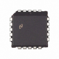
... National does not assume any responsibility for use of any circuitry described no circuit patent licenses are implied and National reserves the right at any time without notice to change said circuitry and specifications 20-Lead PLCC ADC0858BIV or ADC0858CIV NS Package Number V20A 2 A critical component is any component of a life ...