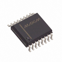
DS1868S-10+ Maxim Integrated Products, DS1868S-10+ Datasheet

DS1868S-10+
Specifications of DS1868S-10+
Related parts for DS1868S-10+
DS1868S-10+ Summary of contents
Page 1
... RST CLK OUT GND DS1868S 16-Pin SOIC (300-mil) PIN DESCRIPTION L0 Low End of Resistor H0 High End of Resistor W0 Wiper Terminal of Resistor S - Stacked Configuration Output OUT - Serial Port Reset Input RST DQ - Serial Port Data Input CLK - Serial Port Clock Input C - Cascade Port Output OUT ...
Page 2
Communication and control of the device is accomplished via a 3-wire serial port interface. This interface allows the ...
Page 3
DS1868 BLOCK DIAGRAM Figure 1 I/O SHIFT REGISTER Figure 2 Transmission of data always begins with the stack select bit followed by the potentiometer-1 wiper position value and lastly the potentiometer-0 wiper position value. When wiper position data is to ...
Page 4
If the stack select bit has value 1, the multiplexed output, S potentiometer-1 wiper DS1868 , will be that of the OUT ...
Page 5
... CASCADE OPERATION A feature of the DS1868 is the ability to control multiple devices from a single processor. Multiple DS1868s can be linked or daisy chained as shown in Figure data bit is entered into the I/O shift register of the DS1868 a bit will appear at the C stack select bit of the DS1868 will always be the first out the part at the beginning of a transaction. The ...
Page 6
ABSOLUTE AND RELATIVE LINEARITY Absolute linearity is defined as the difference between the actual measured output voltage and the expected output voltage. Figure 5 presents the test circuit used to measure absolute linearity. Absolute linearity is given in terms of ...
Page 7
DS1868 ABSOLUTE AND RELATIVE LINEARITY Figure 6 TYPICAL APPLICATION CONFIGURATIONS Figures 7 and 8 show two typical application configurations for the DS1868. By connecting the wiper terminal of the part to a high impedance load, the effects of the wiper ...
Page 8
VARIABLE GAIN AMPLIFIER Figure 7 FIXED GAIN ATTENUATOR Figure DS1868 ...
Page 9
ABSOLUTE MAXIMUM RATINGS* Voltage on Any Pin Relative to Ground (V Voltage on Any Pin when V =-3.3V B Operating Temperature Storage Temperature Soldering Temperature * This is a stress rating only and functional operation of the device at these ...
Page 10
DS1868 ...
Page 11
CAPACITANCE PARAMETER Input Capacitance Output Capacitance AC ELECTRICAL CHARACTERISTICS PARAMETER CLK Frequency Width of CLK Pulse Data Setup Time Data Hold Time Propagation Delay Time Low to High Level Clock to Output Propagation Delay Time High to Low Level High ...
Page 12
TIMING DIAGRAMS Figure 9 (a) 3-Wire Serial Interface General Overview (b) Start of Communication Transaction (c) End of Communication Transaction DS1868 ...
Page 13
DIGITAL OUTPUT LOAD SCHEMATIC Figure 10 TYPICAL SUPPLY CURRENT VS. SERIAL CLOCK RATE Figure DS1868 ...
Page 14
DS1868 20-PIN TSSOP DIM MIN MAX 1. 0. 0.75 1. 0.09 0. 0.50 0. 0.65 BSC B MM 0.18 0. 6.40 6. ...


