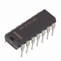
DS1267-010+ Maxim Integrated Products, DS1267-010+ Datasheet

DS1267-010+
Specifications of DS1267-010+
Related parts for DS1267-010+
DS1267-010+ Summary of contents
Page 1
... DIP, 16-pin SOIC, 20-pin TSSOP packages § Resistive elements are temperature compensated to ±0.3 LSB relative linearity § Standard resistance values: – DS1267- – DS1267- – DS1267-100 ~ 100 k § Operating Temperature Range: – Industrial: -40°C to +85°C PIN DESCRIPTIONS L0 Low End of Resistor ...
Page 2
... The DS1267 contains two 256-position potentiometers whose wiper positions are set by an 8-bit value. These two 8-bit values are written to a 17-bit I/O shift register that is used to store the two wiper positions and the stack select bit when the device is powered. A block diagram of the DS1267 is presented in Figure 1. ...
Page 3
... Transmission of data always begins with the stack select bit followed by the potentiometer-1 wiper position value and lastly the potentiometer-0 wiper position value. When wiper position data written to the DS1267, 17 bits (or some integer multiple) of data should always be transmitted. Transactions which do not send a complete 17-bits (or multiple) will leave the register incomplete and possibly an error in the desired wiper positions ...
Page 4
... DS1267s can be linked or daisy-chained as shown in Figure data bit is entered into the I/O shift register of the DS1267 a bit will appear at the C The stack select bit of the DS1267 will always be the first out the part at the beginning of a transaction. Additionally the C pin is always active regardless of the state of OUT shift register without changing its value ...
Page 5
... O O Figure plot of absolute linearity and relative linearity versus wiper position for the DS1267 at 25°C. The specification for absolute linearity of the DS1267 is ±0.75 MI typical. The specification for relative linearity of the DS1267 is ±0.3 MI typical. pin and isolation resistor, the DQ line is left floating by the reading ...
Page 6
... DS1267 ABSOLUTE AND RELATIVE LINEARITY Figure 6 TYPICAL APPLICATION CONFIGURATIONS Figures 7 and 8 show two typical application configurations for theDS1267. By connecting the wiper terminal of the part to a high-impedance load, the effects of the wiper resistance is minimized, since the wiper resistance can vary from 400 to 1000ohms depending on wiper voltage. Figure 7 presents the device connected in an inverting variable gain amplifier ...
Page 7
... INVERTING VARIABLE GAIN AMPLIFIER Figure 7 FIX GAIN ATTENUATOR Figure DS1267 102199 ...
Page 8
... SYMBOL MIN TYP -5.5 B L,H,W V -0 SYMBOL MIN TYP 400 STBY DS1267 =5.0V ±10%) CC MAX UNITS NOTES GND +0 5.0V ± 10%) CC MAX UNITS NOTES 650 µ µA 1000 µ µA 5 102199 ...
Page 9
... SYMBOL MIN TYP OUT (- + SYMBOL MIN TYP f DC CLK CDH t PLH t PHL HLT t 125 RLT 5.0V ± 10%) CC TYP MAX UNITS +20 % ±.75 LDB ±0.3 LDB Hz 750 ppm MAX UNITS 5.0V ± 10%) CC MAX UNITS 10 MHz 102199 DS1267 NOTES =25 C) NOTES NOTES ...
Page 10
... Relative linearity is used to determine the change in voltage between successive tap positions. Device test limits ±0.5 LSB. 5. Typical values are for T = 25°C and nominal supply voltage cutoff frequency characteristics for the DS1267 depend on potentiometer total resistance: DS1267-010: 1 MHz; DS1267-050: 200 kHz; DS1267-100: 100 kHz active regardless of the state of OUT 8 ...
Page 11
... END OF COMMUNICATION TRANSACTION DIGITAL OUTPUT LOAD SCHEMATIC Figure DS1267 102199 ...
Page 12
... TYPICAL SUPPLY CURENT VS. SERIAL CLOCK RATE Figure DS1267 102199 ...


