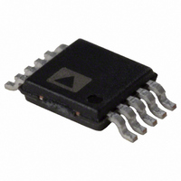
AD5259BRMZ50 Analog Devices Inc, AD5259BRMZ50 Datasheet

AD5259BRMZ50
Specifications of AD5259BRMZ50
Available stocks
Related parts for AD5259BRMZ50
AD5259BRMZ50 Summary of contents
Page 1
FEATURES Nonvolatile memory maintains wiper settings 256-position Thin LFCSP- 0.8 mm) package Compact MSOP- × 4 1.1mm) package I 2 C®-compatible interface V pin provides increased interface flexibility LOGIC End-to-end ...
Page 2
AD5259 TABLE OF CONTENTS Specifications ..................................................................................... 3 Electrical Characteristics ............................................................. 3 Timing Characteristics ................................................................ 5 Absolute Maximum Ratings ............................................................ 6 ESD Caution .................................................................................. 6 Pin Configuration and Function Descriptions ............................. 7 Typical Performance Characteristics ............................................. 8 Test Circuits ..................................................................................... 13 ...
Page 3
SPECIFICATIONS ELECTRICAL CHARACTERISTICS ± 10 ± 10 LOGIC Table 1. Parameter DC CHARACTERISTICS: RHEOSTAT MODE Resistor Differential Nonlinearity 5 kΩ 10 kΩ 50 kΩ/100 kΩ Resistor Integral Nonlinearity 5 ...
Page 4
AD5259 Parameter DIGITAL INPUTS AND OUTPUTS Input Logic High Input Logic Low Leakage Current SDA, AD0, AD1 SCL – Logic High SCL – Logic Low Input Capacitance POWER SUPPLIES Power Supply Range Positive Supply Current Logic Supply Logic Supply Current ...
Page 5
TIMING CHARACTERISTICS ± 10 ± 10 LOGIC Table 2. Parameter INTERFACE TIMING 1 CHARACTERISTICS SCL Clock Frequency t Bus Free Time Between Stop BUF and Start ...
Page 6
AD5259 ABSOLUTE MAXIMUM RATINGS T = 25°C, unless otherwise noted. A Table 3. Parameter GND DD LOGIC GND MAX 1 Pulsed Continuous Digital Inputs and Output ...
Page 7
PIN CONFIGURATION AND FUNCTION DESCRIPTIONS Table 4. Pin Function Descriptions Pin Mnemonic ADO 3 AD1 4 SDA 5 SCL 6 V LOGIC 7 GND AD0 B ...
Page 8
AD5259 TYPICAL PERFORMANCE CHARACTERISTICS 5 kΩ +25°C; unless otherwise noted. DD LOGIC AB A 1.5 1.3 2.7V 1.1 0.9 0.7 0.5 0.3 0.1 –0.1 –0.3 5.5V –0 ...
Page 9
C –40 –0.1 –0.2 –0.3 –0.4 +85 C –0 128 160 192 CODE (Decimal) Figure 12. R-INL vs. Code vs. Temperature 0.5 0.4 0.3 T ...
Page 10
AD5259 400 100k 300 50k 200 10k 100 0 –100 –200 –300 5k –400 –500 –600 128 CODE (Decimal) Figure 18. Rheostat Mode Tempco (Δ 10k 20 100k ...
Page 11
H – – – – – – – –48 –54 –60 1k 10k 100k FREQUENCY (Hz) Figure 24. Gain vs. Frequency vs. Code, R ...
Page 12
AD5259 1s/DIV Figure 30. Midscale Glitch, Code 0×7F to 0× SCL 2 Figure 31. Large Signal Settling Time Rev Page 200ns/DIV ...
Page 13
TEST CIRCUITS Figure 32 through Figure 37 illustrate the test circuits that define the test conditions used in the product Specifications tables DUT 1LSB = V+/ Figure 32. Test Circuit for Potentiometer ...
Page 14
AD5259 THEORY OF OPERATION The AD5259 is a 256-position digitally-controlled variable resistor (VR) device. EEPROM is pre-loaded at midscale from the factory, and initial power-up is, accordingly, at midscale. PROGRAMMING THE VARIABLE RESISTOR Rheostat Operation The nominal resistance (R ) ...
Page 15
I C-COMPATIBLE INTERFACE The master initiates data transfer by establishing a start condi- tion, which is when a high-to-low transition on the SDA line occurs while SCL is high (see Figure 4). The next byte is the slave address ...
Page 16
AD5259 2 I C-COMPATIBLE FORMAT The following generic, write, read, and store/restore control registers for the AD5259 all refer to the device addresses listed in Table 5; the mode/condition reference key (S, P, SA, MA, NA and ...
Page 17
READ MODES Read modes are referred to as traditional because the first two bytes for all three cases are dummy bytes, which function to place the pointer towards the correct register; this is the reason for the repeat start. Theoretically, ...
Page 18
AD5259 TOLERANCE READBACK MODES Table 15. Traditional Readback of Tolerance (Individually) 7-Bit Device Address S (See Table Slave Address Byte Instruction Byte 7-Bit Device Address S (See ...
Page 19
ESD PROTECTION OF DIGITAL PINS AND RESISTOR TERMINALS The AD5259 and GND power supplies define the DD LOGIC boundary conditions for proper 3-terminal and digital input operation. Supply signals present on Terminal A, Terminal B, and ...
Page 20
AD5259 DISPLAY APPLICATIONS CIRCUITRY A special feature of the AD5259 is its unique separation of the V and V supply pins. The separation provides greater LOGIC DD flexibility in applications that do not always provide needed supply voltages. In particular, ...
Page 21
OUTLINE DIMENSIONS IDENTIFIER PIN 1 INDEX AREA 0.80 0.75 0.70 SEATING PLANE 3.10 3.00 2.90 5. 3.10 4.90 3.00 4.65 1 2.90 5 PIN 1 0.50 BSC 0.95 15° MAX 0.85 1.10 MAX 0.75 0.15 0.23 6° 0.30 ...
Page 22
... Model R (Ω) AB AD5259BRMZ5 5 k AD5259BRMZ5- AD5259BCPZ5- AD5259BRMZ10 10 k AD5259BRMZ10- AD5259BCPZ10- AD5259BRMZ50 50 k AD5259BRMZ50- AD5259BCPZ50- AD5259BRMZ100 100 k AD5259BRMZ100-R7 100 k AD5259BCPZ100-R7 100 k AD5259EVAL RoHS Compliant Part. 2 The evaluation board is shipped with the 10 kΩ R Package Description Temperature –40°C to +85°C 10-Lead MSOP – ...
Page 23
NOTES Rev Page AD5259 ...
Page 24
AD5259 NOTES refers to a communications protocol originally developed by Philips Semiconductors (now NXP Semiconductors). ©2005–2010 Analog Devices, Inc. All rights reserved. Trademarks and registered trademarks are the property of their respective companies. D05026-0-5/10(B) Rev ...


