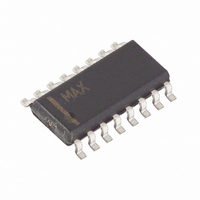
DS1803Z-050 Maxim Integrated Products, DS1803Z-050 Datasheet

DS1803Z-050
Specifications of DS1803Z-050
Related parts for DS1803Z-050
DS1803Z-050 Summary of contents
Page 1
... Addressable Dual Digital Potentiometer PIN ASSIGNMENT GND 7 DS1803 14-PIN TSSOP (173 MIL GND 8 DS1803Z 16-PIN SO (150 MIL) DS1803 16-PIN DIP (300 MIL) See Mech. Drawings Section on Website DS1803 14 VCC SDA 8 SCL 16 VCC SDA 9 SCL ...
Page 2
DEVICE OPERATION The DS1803 is an addressable, digitally controlled device which has two 256-position potentiometers. A functional block diagram of the part is shown in Figure 1. Communication and control of the device is accomplished via a 2-wire serial interface. ...
Page 3
Stop data transfer: A change in the state of the data line, from LOW to HIGH, while the clock line is HIGH, defines the STOP condition. Data valid: The state of the data line represents valid data when, after a ...
Page 4
SLAVE ADDRESS The control byte is the first byte received following the START condition from the master device. The control byte consists of a four bit control code; for the DS1803, this is 0101 binary. The next three bits of ...
Page 5
DS1803. The binary value of each write command is shown in Figure 5 and also in the Table 1. 2-WIRE COMMAND WORDS Table 1 COMMAND Write Potentiometer-0 Write Potentiometer-1 Write Both Potentiometers COMMAND ...
Page 6
ABSOLUTE MAXIMUM RATINGS* Voltage on Any Pin Relative to Ground Operating Temperature Storage Temperature Soldering Temperature * This is a stress rating only and functional operation of the device at these or any other conditions above those indicated in the ...
Page 7
ANALOG RESISTOR CHARACTERISTICS PARAMETER End-to-End Resistor Tolerance Absolute Linearity Relative Linearity -3 dB Cutoff Frequency Temperature Coefficient Capacitance AC ELECTRICAL CHARACTERISTICS PARAMETER SCL Clock Frequency Bus Free Time Between STOP and START Condition Hold Time (Repeated) START Condition Low Period ...
Page 8
After this period, the first clock pulse is generated device must internally provide a hold time of at least 300 ns for the SDA signal (referred to the V of the SCL signal) in order to bridge ...
Page 9
DS1803 BLOCK DIAGRAM Figure 1 2–WIRE DATA TRANSFER OVERVIEW Figure ...
Page 10
CONTROL BYTE Figure 3 2–WIRE READ PROTOCOL Figure 4 2–WIRE WRITE PROTOCOL Figure 5 Write Pot ...
Page 11
... DIP T&R DS1803E-10/T&R 14L TSSOP (173 MIL) T&R DS1803E-50/T&R 14L TSSOP (173 MIL) T&R DS1803E-100/T&R 14L TSSOP (173 MIL) T&R DS1803Z-010/T&R 16L SOIC (150 MIL) T&R DS1803Z-050/T&R 16L SOIC (150 MIL) T&R DS1803Z-100/T&R 16L SOIC (150 MIL) T&R PACKAGE OPERATING VERSION TEMPERATURE -40° ...


