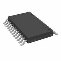
AD5233BRUZ10-R7 Analog Devices Inc, AD5233BRUZ10-R7 Datasheet - Page 16

AD5233BRUZ10-R7
Manufacturer Part Number
AD5233BRUZ10-R7
Description
IC DGTL POT QUAD 64POS 24-TSSOP
Manufacturer
Analog Devices Inc
Datasheet
1.AD5233BRUZ10-R7.pdf
(32 pages)
Specifications of AD5233BRUZ10-R7
Taps
64
Resistance (ohms)
10K
Number Of Circuits
4
Temperature Coefficient
600 ppm/°C Typical
Memory Type
Non-Volatile
Interface
4-Wire SPI Serial
Voltage - Supply
2.7 V ~ 5.5 V, ±2.25 V ~ 2.75 V
Operating Temperature
-40°C ~ 85°C
Mounting Type
Surface Mount
Package / Case
24-TSSOP
Resistance In Ohms
10K
Number Of Elements
4
# Of Taps
64
Resistance (max)
10KOhm
Power Supply Requirement
Single/Dual
Interface Type
Serial (4-Wire/SPI)
Single Supply Voltage (typ)
3/5V
Dual Supply Voltage (typ)
±2.5V
Single Supply Voltage (min)
2.7V
Single Supply Voltage (max)
5.5V
Dual Supply Voltage (min)
±2.25V
Dual Supply Voltage (max)
±2.75V
Operating Temp Range
-40C to 85C
Operating Temperature Classification
Industrial
Mounting
Surface Mount
Pin Count
24
Lead Free Status / RoHS Status
Lead free / RoHS Compliant
AD5233
EEMEM PROTECTION
The write protect ( WP ) pin disables any changes to the
scratchpad register contents, except for the EEMEM setting,
which can still be restored using Instruction 1, Instruction 8,
and the PR pulse. Therefore, WP can be used to provide a
hardware EEMEM protection feature. To disable WP , it is
recommended to execute a NOP instruction before returning
WP to Logic 1.
DIGITAL INPUT/OUTPUT CONFIGURATION
All digital inputs are ESD-protected, high input impedance
that can be driven directly from most digital sources. Active at
Logic 0, PR and WP must be tied to V
No internal pull-up resistors are present on any digital input
pins. Because the device can be detached from the driving
source once it is programmed, adding pull-up resistance on
the digital input pins is a good way to avoid falsely triggering
the floating pins in a noisy environment.
The SDO and RDY pins are open-drain digital outputs that
need pull-up resistors only if these functions are used. Use a
resistor in the range of 1 kΩ to 10 kΩ to balance the power
and switching speed trade-off.
SERIAL DATA INTERFACE
The AD5233 contains a 4-wire SPI-compatible digital interface
(SDI, SDO, CS , and CLK). It uses a 16-bit serial data-word
loaded MSB first. The format of the SPI-compatible word is
shown in
the complete data-word is loaded into the SDI pin. When CS
returns high, the serial data-word is decoded according to the
instructions in
operation of the digital potentiometer. The address bits (Ax)
determine which register is activated. The data bits (Dx) are
the values that are loaded into the decoded register. To program
RDAC1 to RDAC4, only the 6 LSB data bits are used.
The AD5233 has an internal counter that counts a multiple
of 16 bits (a frame) for proper operation. For example, the
AD5233 works with a 32-bit word, but it cannot work properly
with a 15-bit or 17-bit word. In addition, the AD5233 has a
subtle feature that, if CS is pulsed without CLK and SDI, the
part repeats the previous command (except during power-up).
As a result, care must be taken to ensure that no excessive noise
exists in the CLK or CS line that might alter the effective number-
of-bits pattern. Also, to prevent data from locking incorrectly
(due to noise, for example), the counter resets, if the count is
not a multiple of four when CS goes high.
Table 6
Table 7
. The chip-select
. The command bits (Cx) control the
CS pin must be held low until
DD
if they are not used.
Rev. B | Page 16 of 32
The equivalent serial data input and output logic is shown in
Figure 36. The open-drain output SDO is disabled whenever
chip select ( CS ) is in Logic 1. The SPI interface can be used
in two slave modes: CPHA = 1, CPOL = 1 and CPHA = 0,
CPOL = 0. CPHA and CPOL refer to the control bits that
dictate SPI timing in the following MicroConverters® and
microprocessors:
MC68HC16R1/MC68HC916R1. ESD protection of the
digital inputs is shown in
CLK
SDI
CS
LOGIC
Figure 37. Equivalent ESD Digital Input Protection
Figure 36. Equivalent Digital Input-Output Logic
PINS
COUNTER
WP
Figure 38. Equivalent WP Input Protection
COMMAND
VALID
ADuC812 ADuC824
Figure 37
INPUT
REGISTER
300Ω
,
SERIAL
AND ADDRESS
AD5233
INPUT
PROCESSOR
PR
300Ω
COMMAND
DECODE
and
WP
, M68HC11, and
GND
V
Figure 38
DD
GND
V
DD
SDO
GND
5V
.
(FOR DAISY
CHAIN ONLY)
R
PULL-UP


