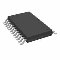
AD5233BRUZ10-R7 Analog Devices Inc, AD5233BRUZ10-R7 Datasheet - Page 26

AD5233BRUZ10-R7
Manufacturer Part Number
AD5233BRUZ10-R7
Description
IC DGTL POT QUAD 64POS 24-TSSOP
Manufacturer
Analog Devices Inc
Datasheet
1.AD5233BRUZ10-R7.pdf
(32 pages)
Specifications of AD5233BRUZ10-R7
Taps
64
Resistance (ohms)
10K
Number Of Circuits
4
Temperature Coefficient
600 ppm/°C Typical
Memory Type
Non-Volatile
Interface
4-Wire SPI Serial
Voltage - Supply
2.7 V ~ 5.5 V, ±2.25 V ~ 2.75 V
Operating Temperature
-40°C ~ 85°C
Mounting Type
Surface Mount
Package / Case
24-TSSOP
Resistance In Ohms
10K
Number Of Elements
4
# Of Taps
64
Resistance (max)
10KOhm
Power Supply Requirement
Single/Dual
Interface Type
Serial (4-Wire/SPI)
Single Supply Voltage (typ)
3/5V
Dual Supply Voltage (typ)
±2.5V
Single Supply Voltage (min)
2.7V
Single Supply Voltage (max)
5.5V
Dual Supply Voltage (min)
±2.25V
Dual Supply Voltage (max)
±2.75V
Operating Temp Range
-40C to 85C
Operating Temperature Classification
Industrial
Mounting
Surface Mount
Pin Count
24
Lead Free Status / RoHS Status
Lead free / RoHS Compliant
AD5233
PROGRAMMABLE OSCILLATOR
In a classic Wien-bridge oscillator, shown in Figure 55, the
Wien network (R, R´, C, C´) provides positive feedback, while
R1 and R2 provide negative feedback. At the resonant frequency,
f
causes the circuit to oscillate. If the op amp is chosen with a
relatively high gain bandwidth product, the frequency response
of the op amp can be neglected.
With R = R´, C = C´, and R2 = R2A||(R2B + R
oscillation frequency is
where R is equal to R
At resonance, setting
balances the bridge. In practice, R2/R1 should be set slightly
larger than 2 to ensure that the oscillation can start. On the
other hand, the alternate turn-on of the diodes, D1 and D2,
ensures that R1/R2 is smaller than 2 momentarily and,
therefore, stabilizes the oscillation.
Once the frequency is set, the oscillation amplitude can be
turned on by R2B, because
where V
With proper selection of R2B, an equilibrium is reached such
that V
to increase the amplitude, but the total resistance cannot be too
large or it saturates the output. In this configuration, R2B can be
adjusted from minimum to full scale with amplitude varied
from ±0.6 V to ±0.9 V. Using 2.2 nF for C and C´, 10 kΩ dual
O
, the overall phase shift is zero, and the positive feedback
ω
R
R2
2
3
R1
O
O
Figure 55. Programmable Oscillator with Amplitude Control
V
=
R = R' = R2B = 1/4 AD5233
D1 = D2 = 1N4148
converges. R2B can be in series with a discrete resistor
O
O
=
2.2nF
=
, I
64 −
2
=
D
64
RC
C
, and V
1
I
D
D
or
R2B
R
10kΩ
ADJUSTMENT
FREQUENCY
AB
D
f
O
R
+
WA
are interdependent variables.
B
A
V
=
such that
D
2
W
1kΩ
VN
π
R1
1
RC
VP
B
10kΩ
R2B
W
OP1177
+2.5V
–2.5V
2.2nF
C'
A
V+
V–
ADJUSTMENT
2.1kΩ
R2A
AMPLITUDE
A
U1
10kΩ
W
R'
B
D1
D2
DIODE
), the
V
O
(13)
(14)
(15)
(16)
Rev. B | Page 26 of 32
digital potentiometer, with R and R´ set to 8.06 kΩ, 4.05 kΩ,
and 670 Ω, oscillation occurs at 8.8 kHz, 17.6 kHz, and
102 kHz, respectively (see Figure 56).
In both circuits (shown in Figure 51 and Figure 55), the
frequency tuning requires that both RDACs be adjusted to
the same settings. Because the two channels might be adjusted
one at a time, an intermediate state occurs that might not be
acceptable for some applications. Of course, the increment/
decrement all instructions (5, 7, 13, and 15) can be used.
Different devices can also be used in daisy-chain mode so that
parts can be programmed to the same setting simultaneously.
PROGRAMMABLE VOLTAGE SOURCE WITH
BOOSTED OUTPUT
For applications that require high current adjustment, such as a
laser diode driver or tunable laser, a boosted voltage source can
be considered (see Figure 57).
In this circuit, the inverting input of the op amp forces the V
to be equal to the wiper voltage set by the digital potentiometer.
The load current is then delivered by the supply via the N-
channel FET N
dissipate (V
maximum of 100 mA with a 5 V supply.
For precision applications, a voltage reference such as ADR421,
ADR03, or ADR370 can be applied at Terminal A of the digital
potentiometer.
1V/DIV
1V/DIV
1V/DIV
V
IN
A
Figure 57. Programmable Boosted Voltage Source
B
i
AD5233
− V
W
1
. N
O
Figure 56. Programmable Oscillation
) × I
AD8601
1
U2
power handling must be adequate to
L
power. This circuit can source a
V+
V–
2N7002
SIGNAL
LD
C
C
R
V
R = 8.06kΩ
f = 8.8kHz
R = 4.05kΩ
f = 17.6kHz
R = 670Ω
f = 102kHz
BIAS
OUT
I
L
OUT


