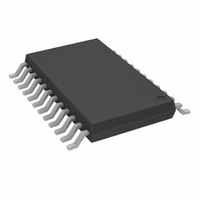
AD5233BRUZ10-R7 Analog Devices Inc, AD5233BRUZ10-R7 Datasheet - Page 5

AD5233BRUZ10-R7
Manufacturer Part Number
AD5233BRUZ10-R7
Description
IC DGTL POT QUAD 64POS 24-TSSOP
Manufacturer
Analog Devices Inc
Datasheet
1.AD5233BRUZ10-R7.pdf
(32 pages)
Specifications of AD5233BRUZ10-R7
Taps
64
Resistance (ohms)
10K
Number Of Circuits
4
Temperature Coefficient
600 ppm/°C Typical
Memory Type
Non-Volatile
Interface
4-Wire SPI Serial
Voltage - Supply
2.7 V ~ 5.5 V, ±2.25 V ~ 2.75 V
Operating Temperature
-40°C ~ 85°C
Mounting Type
Surface Mount
Package / Case
24-TSSOP
Resistance In Ohms
10K
Number Of Elements
4
# Of Taps
64
Resistance (max)
10KOhm
Power Supply Requirement
Single/Dual
Interface Type
Serial (4-Wire/SPI)
Single Supply Voltage (typ)
3/5V
Dual Supply Voltage (typ)
±2.5V
Single Supply Voltage (min)
2.7V
Single Supply Voltage (max)
5.5V
Dual Supply Voltage (min)
±2.25V
Dual Supply Voltage (max)
±2.75V
Operating Temp Range
-40C to 85C
Operating Temperature Classification
Industrial
Mounting
Surface Mount
Pin Count
24
Lead Free Status / RoHS Status
Lead free / RoHS Compliant
TIMING CHARACTERISTICS
V
Table 2.
Parameter
INTERFACE TIMING CHARACTERISTICS
FLASH/EE MEMORY RELIABILITY
1
2
3
4
5
6
7
8
Typicals represent average readings at 25°C and V
Guaranteed by design and not subject to production test.
See the timing diagrams (Figure 2 and Figure 3) for the location of the measured values. All input control voltages are specified with t
and timed from a voltage level of 1.5 V. Switching characteristics are measured using both V
Propagation delay depends on the value of V
Valid for commands that do not activate the RDY pin.
The RDY pin is low only for Command 2, Command 3, Command 8, Command 9, Command 10, and the PR hardware pulse: CMD_8 > 1 ms; CMD_9, CMD_10 > 0.12 ms;
CMD_2, CMD_3 > 20 ms. Device operation at T
Endurance is qualified to 100,000 cycles per JEDEC Standard 22, Method A117, and measured at −40°C, +25°C, and +85°C; typical endurance at 25°C is 700,000 cycles.
Retention lifetime equivalent at junction temperature (T
derates with junction temperature, as shown in Figure 45 in the Flash/EEMEM Reliability section.
DD
Clock Cycle Time (t
CS Setup Time
CLK Shutdown Time to CS Rise
Input Clock Pulse Width
Data Setup Time
Data Hold Time
CS to SDO-SPI Line Acquire
CS to SDO-SPI Line Release
CLK to SDO Propagation Delay
CLK to SDO Data Hold Time
CS High Pulse Width
CS High to CS High
RDY Rise to CS Fall
CS Rise to RDY Fall Time
Read/Store to Nonvolatile EEMEM
CS Rise to Clock Rise/Fall Setup
Preset Pulse Width (Asynchronous)
Preset Response Time to Wiper Setting
Power-On EEMEM Restore Time
Endurance
Data Retention
= 3 V to 5.5 V, V
7
8
CYC
SS
5
5
= 0 V, and −40°C < T
)
4
6
2, 3
DD
A
, R
= −40°C and V
PULL-UP
DD
A
= 5 V.
Symbol
t
t
t
t
t
t
t
t
t
t
t
t
t
t
t
t
t
t
t
1
2
3
4
6
7
8
9
10
11
12
13
14
15
16
17
PRW
PRESP
EEMEM1
< +85°C, unless otherwise noted.
, t
, and C
J
5
) = 55°C per JEDEC Standard 22, Method A117. Retention lifetime based on an activation energy of 0.6 eV
L
.
DD
< 3 V extends the save time to 35 ms.
Conditions
Clock level high or low
From positive CLK transition
From positive CLK transition
R
R
Applies to Instruction 0x2, Instruction 0x3,
and Instruction 0x9
Not shown in timing diagram
PR pulsed low to refresh wiper positions
R
PULL-UP
P
AB
= 2.2 kΩ, C
= 10 kΩ
Rev. B | Page 5 of 32
= 2.2 kΩ, C
L
< 20 pF
L
< 20 pF
DD
= 3 V and V
DD
= 5 V.
Min
20
10
1
10
5
5
0
10
4
0
10
50
100
R
= t
Typ
0.1
25
70
140
100
F
= 2.5 ns (10% to 90% of 3 V)
1
Max
40
50
50
0.15
AD5233
Unit
ns
ns
t
ns
ns
ns
ns
ns
ns
ns
ns
t
ns
ms
ms
ns
ns
μs
μs
kCycles
Years
CYC
CYC


