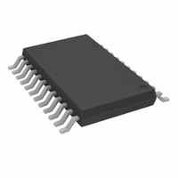
AD5233BRUZ50-R7 Analog Devices Inc, AD5233BRUZ50-R7 Datasheet - Page 17

AD5233BRUZ50-R7
Manufacturer Part Number
AD5233BRUZ50-R7
Description
IC DGTL POT QUAD 64POS 24-TSSOP
Manufacturer
Analog Devices Inc
Datasheet
1.AD5233BRUZ10-R7.pdf
(32 pages)
Specifications of AD5233BRUZ50-R7
Taps
64
Resistance (ohms)
50K
Number Of Circuits
4
Temperature Coefficient
600 ppm/°C Typical
Memory Type
Non-Volatile
Interface
4-Wire SPI Serial
Voltage - Supply
2.7 V ~ 5.5 V, ±2.25 V ~ 2.75 V
Operating Temperature
-40°C ~ 85°C
Mounting Type
Surface Mount
Package / Case
24-TSSOP
Resistance In Ohms
50K
Number Of Elements
4
# Of Taps
64
Resistance (max)
50KOhm
Power Supply Requirement
Single/Dual
Interface Type
Serial (4-Wire/SPI)
Single Supply Voltage (typ)
3/5V
Dual Supply Voltage (typ)
±2.5V
Single Supply Voltage (min)
2.7V
Single Supply Voltage (max)
5.5V
Dual Supply Voltage (min)
±2.25V
Dual Supply Voltage (max)
±2.75V
Operating Temp Range
-40C to 85C
Operating Temperature Classification
Industrial
Mounting
Surface Mount
Pin Count
24
Lead Free Status / RoHS Status
Lead free / RoHS Compliant
DAISY-CHAIN OPERATION
The serial data output (SDO) pin serves two purposes. It can
be used to read the contents of the wiper setting and EEMEM
values using Instruction 10 and Instruction 9, respectively.
The remaining instructions (0 to 8, 11 to 15) are valid for
daisy-chaining multiple devices in simultaneous operations.
Daisy-chaining minimizes the number of port pins required
from the controlling IC (Figure 39). The SDO pin contains an
open-drain N-channel FET that requires a pull-up resistor, if
this function is used. As shown in Figure 39, users need to tie
the SDO pin of one package to the SDI pin of the next package.
Users might need to increase the clock period, because the
pull-up resistor and the capacitive loading at the SDO to SDI
interface might require an additional time delay between
subsequent packages. When two AD5233s are daisy-chained,
32 bits of data is required. The first 16 bits go to U2 and the
second 16 bits go to U1. CS should be kept low until all 32 bits
are clocked into their respective serial registers. CS is then
pulled high to complete the operation.
TERMINAL VOLTAGE OPERATION RANGE
The AD5233’s positive V
define the boundary conditions for proper 3-terminal digital
potentiometer operation. Supply signals present on Terminal A,
Terminal B, and Terminal W that exceed V
by the internal forward-biased diodes (see Figure 40).
CONTROLLER
MICRO-
Figure 40. Maximum Terminal Voltages Set by V
Figure 39. Daisy-Chain Configuration Using SDO
SDI
CS
AD5233
U1
DD
CLK
and negative V
SDO
+V
R
2kΩ
P
DD
SDI
SS
CS
or V
power supplies
AD5233
SS
U2
DD
V
A
W
V
B
are clamped
SS
DD
and V
CLK
SDO
SS
Rev. B | Page 17 of 32
The ground pin of the AD5233 device is used primarily as a
digital ground reference, which needs to be tied to the PCB’s
common ground. The digital input control signals to the
AD5233 must be referenced to the device ground pin (GND)
and satisfy the logic level defined in the Specifications section.
An internal level-shift circuit ensures that the common-mode
voltage range of the three terminals extends from V
regardless of the digital input level.
POWER-UP SEQUENCE
Because there are diodes to limit the voltage compliance at
Terminal A, Terminal B, and Terminal W (see Figure 40), it is
important to power on V
to Terminal A, Terminal B, and Terminal W. Otherwise, the
diode is forward-biased such that V
tentionally. For example, applying 5 V across the A and B
terminals prior to V
It is not destructive to the device, but it might affect the rest of
the system. The ideal power-up sequence is GND, V
digital inputs, and V
V
powered after V
Regardless of the power-up sequence and the ramp rates of the
power supplies, once V
remains effective, which restores the EEMEM values to the
RDAC registers.
LATCHED DIGITAL OUTPUTS
A pair of digital outputs, O1 and O2, is available on the AD5233.
These outputs provide a nonvolatile Logic 0 or Logic 1 setting.
O1 and O2 are standard CMOS logic outputs, shown in Figure 41.
These outputs are ideal to replace the functions often provided
by DIP switches. In addition, they can be used to drive other
standard CMOS logic-controlled parts that need an occasional
setting change. Pin O1 and Pin O2 default to Logic 1, and they
can drive up to 50 mA of load at 5 V/25°C.
W
, and digital inputs is not important as long as they are
Figure 41. Logic Output O1 and Logic Output O2
DD
/V
GND
V
DD
A
DD
SS
/V
.
causes the V
DD
B
/V
DD
/V
/V
W
SS
. The order of powering V
OUTPUTS
SS
are powered, the power-on preset
first before applying any voltage
DD
DD
/V
terminal to exhibit 4.3 V.
SS
are powered unin-
O1 AND O2
PINS
SS
AD5233
DD
to V
, V
A
, V
SS
DD
,
B
,
,


