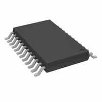
AD5233BRUZ50-R7 Analog Devices Inc, AD5233BRUZ50-R7 Datasheet - Page 22

AD5233BRUZ50-R7
Manufacturer Part Number
AD5233BRUZ50-R7
Description
IC DGTL POT QUAD 64POS 24-TSSOP
Manufacturer
Analog Devices Inc
Datasheet
1.AD5233BRUZ10-R7.pdf
(32 pages)
Specifications of AD5233BRUZ50-R7
Taps
64
Resistance (ohms)
50K
Number Of Circuits
4
Temperature Coefficient
600 ppm/°C Typical
Memory Type
Non-Volatile
Interface
4-Wire SPI Serial
Voltage - Supply
2.7 V ~ 5.5 V, ±2.25 V ~ 2.75 V
Operating Temperature
-40°C ~ 85°C
Mounting Type
Surface Mount
Package / Case
24-TSSOP
Resistance In Ohms
50K
Number Of Elements
4
# Of Taps
64
Resistance (max)
50KOhm
Power Supply Requirement
Single/Dual
Interface Type
Serial (4-Wire/SPI)
Single Supply Voltage (typ)
3/5V
Dual Supply Voltage (typ)
±2.5V
Single Supply Voltage (min)
2.7V
Single Supply Voltage (max)
5.5V
Dual Supply Voltage (min)
±2.25V
Dual Supply Voltage (max)
±2.75V
Operating Temp Range
-40C to 85C
Operating Temperature Classification
Industrial
Mounting
Surface Mount
Pin Count
24
Lead Free Status / RoHS Status
Lead free / RoHS Compliant
AD5233
The EEMEM1 value for RDAC1 can be restored by power-on,
by strobing the PR pin, or by programming, as shown in
Table 14. Restoring the EEMEM1 Value to the
RDAC1 Register
SDI
0x10XX
0x00XX
Table 15. Using Left-Shift by One to Increment 6 dB Step
SDI
0xC0XX
Table 16. Storing Additional User Data in EEMEM
SDI
0x35AA
0x3655
Table 17. Reading Back Data from Memory Locations
SDI
0x95XX
0x00XX
Table 18. Reading Back Wiper Settings
SDI
0xB020
0xC0XX
0xA0XX
0xXXXX
FLASH/EEMEM RELIABILITY
The Flash/EE memory array on the AD5233 is fully qualified
for two key Flash/EE memory characteristics, Flash/EE memory
cycling endurance, and Flash/EE memory data retention.
SDO
0xXXXX
0xB020
0xC0XX
0xA03F
SDO
0xXXXX
0x10XX
SDO
0xXXXX
0x95AA
SDO
0xXXXX
SDO
0xXXXX
0x35AA
Reads back full-scale value from SDO.
Action
Writes RDAC1 to midscale.
Doubles RDAC1 from midscale to full scale
(left-shift instruction).
Prepares reading the wiper setting from the
RDAC1 register.
Action
Restores the EEMEM1 value to the
RDAC1 register.
NOP. Recommended step to minimize
power consumption.
Action
Moves the wiper to double the present
data contained in the RDAC1 register.
Action
Stores Data 0xAA in the extra EEMEM6
location, USER1. (Allowable to address
in 11 locations with a maximum of
eight bits of data.)
Stores Data 0x55 in the extra EEMEM7
location USER2. (Allowable to address
in 11 locations with a maximum of
eight bits of data.)
Action
Prepares data read from USER1 EEMEM
location.
NOP Instruction 0 sends a 16-bit word
out of SDO, where the last eight bits
contain the contents of the USER1
location. The NOP command ensures
that the device returns to the idle
power dissipation state.
Table 14
Rev. B | Page 22 of 32
.
Endurance quantifies the ability of the Flash/EE memory to be
cycled through many program, read, and erase cycles. In real
terms, a single endurance cycle is composed of the following
four independent, sequential events:
•
•
•
•
During reliability qualification, Flash/EE memory is cycled
from 0x00 to 0x3F until a first fail is recorded, signifying the
endurance limit of the on-chip Flash/EE memory.
As indicated in the Specifications section, the AD5233
Flash/EE memory endurance qualification has been carried
out in accordance with JEDEC Specification A117 over the
industrial temperature range of −40°C to +85°C. The results
allow the specification of a minimum endurance figure over
supply and temperature of 100,000 cycles, with an endurance
figure of 700,000 cycles being typical of operation at 25°C.
Retention quantifies the ability of the Flash/EE memory to
retain its programmed data over time. Again, the AD5233 has
been qualified in accordance with the formal JEDEC Retention
Lifetime Specification (A117) at a specific junction temperature
(T
Flash/EE memory is cycled to its specified endurance limit,
described previously, before data retention is characterized.
This means that the Flash/EE memory is guaranteed to retain
its data for its full specified retention lifetime every time the
Flash/EE memory is reprogrammed. It should also be noted
that retention lifetime, based on an activation energy of 0.6 eV,
derates with T
retained for 100 years at 55°C operation, but reduces to 15 years
at 85°C operation. Beyond these limits, the part must be
reprogrammed so that the data can be restored.
J
= 55°C). As part of this qualification procedure, the
Initial page erase sequence
Read/verify sequence
Byte program sequence
Second read/verify sequence
300
250
200
150
100
50
0
40
Figure 45. Flash/EE Memory Data Retention
J
50
as shown in Figure 45. For example, the data is
T
J
60
ANALOG DEVICES
TYPICAL PERFORMANCE
AT T
JUNCTION TEMPERATURE (°C)
J
= 55°C
70
80
90
100
110


