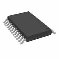
AD5233BRUZ50-R7 Analog Devices Inc, AD5233BRUZ50-R7 Datasheet - Page 8

AD5233BRUZ50-R7
Manufacturer Part Number
AD5233BRUZ50-R7
Description
IC DGTL POT QUAD 64POS 24-TSSOP
Manufacturer
Analog Devices Inc
Datasheet
1.AD5233BRUZ10-R7.pdf
(32 pages)
Specifications of AD5233BRUZ50-R7
Taps
64
Resistance (ohms)
50K
Number Of Circuits
4
Temperature Coefficient
600 ppm/°C Typical
Memory Type
Non-Volatile
Interface
4-Wire SPI Serial
Voltage - Supply
2.7 V ~ 5.5 V, ±2.25 V ~ 2.75 V
Operating Temperature
-40°C ~ 85°C
Mounting Type
Surface Mount
Package / Case
24-TSSOP
Resistance In Ohms
50K
Number Of Elements
4
# Of Taps
64
Resistance (max)
50KOhm
Power Supply Requirement
Single/Dual
Interface Type
Serial (4-Wire/SPI)
Single Supply Voltage (typ)
3/5V
Dual Supply Voltage (typ)
±2.5V
Single Supply Voltage (min)
2.7V
Single Supply Voltage (max)
5.5V
Dual Supply Voltage (min)
±2.25V
Dual Supply Voltage (max)
±2.75V
Operating Temp Range
-40C to 85C
Operating Temperature Classification
Industrial
Mounting
Surface Mount
Pin Count
24
Lead Free Status / RoHS Status
Lead free / RoHS Compliant
AD5233
PIN CONFIGURATION AND FUNCTION DESCRIPTIONS
Table 4. Pin Function Descriptions
Pin No.
1
2
3
4
5
6
7
8
9
10
11
12
13
14
15
16
17
18
19
20
21
22
23
24
Mnemonic
O1
CLK
SDI
SDO
GND
V
A1
W1
B1
A2
W2
B2
B3
W3
A3
B4
W4
A4
V
WP
PR
CS
RDY
O2
SS
DD
Description
Nonvolatile Digital Output 1. Address (O1) = 0x4, the data bit position is D0; defaults to Logic 1 initially.
Serial Input Register Clock Pin. Shifts in one bit at a time on positive clock edges.
Serial Data Input Pin. Shifts in one bit at a time on positive CLK edges. MSB loaded first.
Serial Data Output Pin. Serves readback and daisy-chain functions.
Command 9 and Command 10 activate the SDO output for the readback function, delayed by 16 or 17 clock
pulses, depending on the clock polarity before and after the data-word (see Figure 2, Figure 3, and Table 7).
In other commands, the SDO shifts out the previously loaded SDI bit pattern, delayed by 16 or 17 clock pulses,
depending on the clock polarity (see Figure 2 and Figure 3). This previously shifted-out SDI can be used for daisy-
chaining multiple devices.
Whenever SDO is used, a pull-up resistor in the range of 1 kΩ to 10 kΩ is needed.
Ground Pin, Logic Ground Reference.
Negative Supply. Connect to 0 V for single-supply applications. If V
40 mA for 25 ms when storing data to EEMEM.
Terminal A of RDAC1.
Wiper Terminal of RDAC1, Address (RDAC1) = 0x0.
Terminal B of RDAC1.
Terminal A of RDAC2.
Wiper Terminal of RDAC2, Address (RDAC2) = 0x1.
Terminal B of RDAC2.
Terminal B of RDAC3.
Wiper Terminal of RDAC3, Address (RDAC3) = 0x2.
Terminal A of RDAC3.
Terminal B of RDAC4.
Wiper Terminal of RDAC4, Address (RDAC4) = 0x3.
Terminal A of RDAC4.
Positive Power Supply Pin.
Optional Write Protect Pin. When active low, WP prevents any changes to the present contents, except PR strobe
and Instruction 1 and Instruction 8, and refreshes the RDAC register from EEMEM. Execute a NOP instruction
before returning to WP high. Tie WP to V
Optional Hardware Override Preset Pin. Refreshes the scratchpad register with current contents of the EEMEM
register. Factory default loads midscale 0x20 until EEMEM is loaded with a new value by the user. PR is activated at
the Logic 1 transition. Tie PR to V
Serial Register Chip Select Active Low. Serial register operation takes place when CS returns to Logic 1.
Ready. Active-high open-drain output. Identifies completion of Software Instruction 2, Software Instruction 3,
Software Instruction 8, Software Instruction 9, Software Instruction 10, and Hardware Instruction PR.
Nonvolatile Digital Output 2. Address (O2) = 0x4, the data bit position is D1; defaults to Logic 1 initially.
GND
SDO
CLK
V
SDI
W1
W2
O1
A1
B1
A2
B2
SS
DD
Figure 4. Pin Configuration
10
11
12
if not used.
1
2
3
4
5
6
7
8
9
Rev. B | Page 8 of 32
(Not to Scale)
AD5233
TOP VIEW
DD
if not used.
24
23
22
21
20
19
18
17
16
15
14
13
O2
RDY
CS
PR
WP
A4
W4
B4
A3
W3
B3
V
DD
SS
is used in dual supply, it must be able to sink


