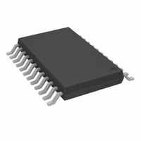
AD8403ARU100-REEL Analog Devices Inc, AD8403ARU100-REEL Datasheet - Page 20

AD8403ARU100-REEL
Manufacturer Part Number
AD8403ARU100-REEL
Description
IC POT DIG QUAD 100K 8B 24TSSOP
Manufacturer
Analog Devices Inc
Datasheet
1.AD8400ARZ1.pdf
(32 pages)
Specifications of AD8403ARU100-REEL
Rohs Status
RoHS non-compliant
Taps
256
Resistance (ohms)
100K
Number Of Circuits
4
Temperature Coefficient
500 ppm/°C Typical
Memory Type
Volatile
Interface
SPI, 3-Wire Serial
Voltage - Supply
2.7 V ~ 5.5 V
Operating Temperature
-40°C ~ 125°C
Mounting Type
Surface Mount
Package / Case
24-TSSOP
Resistance In Ohms
100K
Number Of Elements
4
# Of Taps
256
Resistance (max)
100KOhm
Power Supply Requirement
Single
Interface Type
Serial (3-Wire/SPI)
Single Supply Voltage (typ)
3/5V
Dual Supply Voltage (typ)
Not RequiredV
Single Supply Voltage (min)
2.7V
Single Supply Voltage (max)
5.5V
Dual Supply Voltage (min)
Not RequiredV
Dual Supply Voltage (max)
Not RequiredV
Operating Temp Range
-40C to 125C
Operating Temperature Classification
Automotive
Mounting
Surface Mount
Pin Count
24
Package Type
TSSOP
For Use With
AD8403EVAL - BOARD EVAL FOR AD8403
Lead Free Status / Rohs Status
Not Compliant
Available stocks
Company
Part Number
Manufacturer
Quantity
Price
Company:
Part Number:
AD8403ARU100-REEL
Manufacturer:
A/D
Quantity:
280
Part Number:
AD8403ARU100-REEL
Manufacturer:
ADI/亚德诺
Quantity:
20 000
AD8400/AD8402/AD8403
THEORY OF OPERATION
The AD8400/AD8402/AD8403 provide a single, dual, and quad
channel, 256-position, digitally controlled variable resistor (VR)
device. Changing the programmed VR setting is accomplished
by clocking in a 10-bit serial data-word into the SDI (Serial
Data Input) pin. The format of this data-word is two address
bits, MSB first, followed by eight data bits, also MSB first.
Table 6 provides the serial register data-word format. The
AD8400/AD8402/AD8403 have the following address assign-
ments for the ADDR decoder, which determines the location
of the VR latch receiving the serial register data in Bit B7 to
Bit B0:
The single-channel AD8400 requires A1 = A0 = 0. The dual-
channel AD8402 requires A1 = 0. VR settings can be changed
one at a time in random sequence. A serial clock running at
10 MHz makes it possible to load all four VRs under 4 μs
(10 × 4 × 100 ns) for AD8403. The exact timing requirements
are shown in Figure 3, Figure 4, and Figure 5.
The AD8400/AD8402/AD8403 do not have power-on midscale
preset, so the wiper can be at any random position at power-up.
However, the AD8402/AD8403 can be reset to midscale by
asserting the RS pin, simplifying initial conditions at power-up.
Both parts have a power shutdown SHDN pin that places the
VR in a zero-power-consumption state where Terminal Ax is
open-circuited and the Wiper Wx is connected to Terminal Bx,
resulting in the consumption of only the leakage current in the
VR. In shutdown mode, the VR latch settings are maintained
so that upon returning to the operational mode, the VR settings
return to the previous resistance values. The digital interface is
still active in shutdown, except that SDO is deactivated. Code
changes in the registers can be made during shutdown that will
produce new wiper positions when the device is taken out of
shutdown.
VR# = A1 × 2 + A0 + 1
Figure 45. AD8402/AD8403 Equivalent VR (RDAC) Circuit
SHDN
D7
D6
D5
D4
D3
D2
D1
D0
DECODER
LATCH
RDAC
AND
R
R
R
R
S
S
S
S
R
S
= R
NOMINAL
/256
Ax
Wx
Bx
Rev. E | Page 20 of 32
(1)
PROGRAMMING THE VARIABLE RESISTOR
Rheostat Operation
The nominal resistance of the VR (RDAC) between Terminal A
and Terminal B is available with values of 1 kΩ, 10 kΩ, 50 kΩ,
and 100 kΩ. The final digits of the part number determine the
nominal resistance value; that is, 10 kΩ = 10; 100 kΩ = 100.
The nominal resistance (R
accessible by the wiper terminal, and the resulting resistance
can be measured either across the wiper and B terminals (R
or across the wiper and A terminals (R
loaded into the RDAC latch is decoded to select one of the
256 possible settings. The wiper’s first connection starts at the
B terminal for data 00
contact resistance of 50 Ω. The second connection (for the 10 kΩ
part) is the first tap point located at 89 Ω = [R
resistance) + R
connection is the next tap point representing 78 Ω + 50 Ω =
128 Ω for data 02
wiper up the resistor ladder until the last tap point is reached at
10,011 Ω. Note that the wiper does not directly connect to the
B terminal even for data 00
diagram of the equivalent RDAC circuit.
The AD8400 contains one RDAC, the AD8402 contains
two independent RDACs, and the AD8403 contains four
independent RDACs. The general transfer equation that
determines the digitally programmed output resistance
between Wx and Bx is
where D, in decimal, is the data loaded into the 8-bit RDAC#
latch, and R
For example, when the A terminal is either open-circuited or
tied to the Wiper W, the following RDAC latch codes result in
the following R
Table 10.
D (Dec)
255
128
1
0
Note that in the zero-scale condition, a finite wiper resistance of
50 Ω is present. Care should be taken to limit the current flow
between W and B in this state to a maximum value of 5 mA to
avoid degradation or possible destruction of the internal switch
contact.
R
WB
AB
R
10,011
5,050
89
50
WB
( )
is the nominal end-to-end resistance.
W
D
WB
(Ω)
= 39 Ω + 50 Ω] for data 01
H
(for the 10 kΩ version):
. Each LSB data value increase moves the
=
256
H
D
. This B terminal connection has a wiper
Output State
Full scale
Midscale ( RS = 0 condition)
1 LSB
Zero-scale (wiper contact resistance)
×
AB
H
) of the VR has 256 contact points
. See Figure 45 for a simplified
R
AB
+
R
W
WA
). The 8-bit data-word
H
. The third
AB
(nominal
WB
(2)
)


