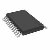
AD8403ARU100-REEL Analog Devices Inc, AD8403ARU100-REEL Datasheet - Page 22

AD8403ARU100-REEL
Manufacturer Part Number
AD8403ARU100-REEL
Description
IC POT DIG QUAD 100K 8B 24TSSOP
Manufacturer
Analog Devices Inc
Datasheet
1.AD8400ARZ1.pdf
(32 pages)
Specifications of AD8403ARU100-REEL
Rohs Status
RoHS non-compliant
Taps
256
Resistance (ohms)
100K
Number Of Circuits
4
Temperature Coefficient
500 ppm/°C Typical
Memory Type
Volatile
Interface
SPI, 3-Wire Serial
Voltage - Supply
2.7 V ~ 5.5 V
Operating Temperature
-40°C ~ 125°C
Mounting Type
Surface Mount
Package / Case
24-TSSOP
Resistance In Ohms
100K
Number Of Elements
4
# Of Taps
256
Resistance (max)
100KOhm
Power Supply Requirement
Single
Interface Type
Serial (3-Wire/SPI)
Single Supply Voltage (typ)
3/5V
Dual Supply Voltage (typ)
Not RequiredV
Single Supply Voltage (min)
2.7V
Single Supply Voltage (max)
5.5V
Dual Supply Voltage (min)
Not RequiredV
Dual Supply Voltage (max)
Not RequiredV
Operating Temp Range
-40C to 125C
Operating Temperature Classification
Automotive
Mounting
Surface Mount
Pin Count
24
Package Type
TSSOP
For Use With
AD8403EVAL - BOARD EVAL FOR AD8403
Lead Free Status / Rohs Status
Not Compliant
Available stocks
Company
Part Number
Manufacturer
Quantity
Price
Company:
Part Number:
AD8403ARU100-REEL
Manufacturer:
A/D
Quantity:
280
Part Number:
AD8403ARU100-REEL
Manufacturer:
ADI/亚德诺
Quantity:
20 000
AD8400/AD8402/AD8403
Table 12. Input Logic Control Truth Table
CLK
L
P
X
X
X
X
X
1
The serial data output (SDO) pin, which exists only on the
AD8403 and not on the AD8400 or AD8402, contains an
open-drain, n-channel FET that requires a pull-up resistor to
transfer data to the SDI pin of the next package. The pull-up
resistor termination voltage may be larger than the V
(but less than the max V
device. For example, the AD8403 could operate at V
and the pull-up for interface to the next device could be set at 5 V.
This allows for daisy-chaining several RDACs from a single proc-
essor serial data line. The clock period needs to be increased
when using a pull-up resistor to the SDI pin of the following
device in the series. Capacitive loading at the daisy-chain node
SDO to SDI between devices must be accounted for in order to
transfer data successfully. When daisy chain is used, CS should
be kept low until all the bits of every package are clocked into
their respective serial registers and the address and data bits are
in the proper decoding location.
SHDN
SDO
P = positive edge, X = don’t care, SR = shift register
CLK
SDI
CS
CS
L
L
P
H
X
H
H
DGND
DO
DI
SER
REG
RS
H
H
H
H
L
P
H
A1
A0
D7
D0
8
Figure 48. AD8403 Block Diagram
SHDN
H
H
H
H
H
H
L
ADDR
DEC
EN
RS
DD
Register Activity
No SR effect; enables SDO pin
Shift one bit in from the SDI pin. The
10th previously entered bit is shifted
out of the SDO pin.
Load SR data into RDAC latch based
on A1, A0 decode (Table 13).
No operation
Sets all RDAC latches to midscale,
wiper centered, and SDO latch
cleared
Latches all RDAC latches to 80
Open-circuits all Resistor A terminals,
connects W to B, turns off SDO
output transistor.
of 8 V) of the AD8403 SDO output
D7
D0
D7
D0
LATCH
LATCH
RDAC
RDAC
NO. 1
NO. 4
R
R
AD8403
AGND
1
DD
DD
V
A1
W1
B1
A4
W4
B4
DD
supply
= 3.3 V,
H
Rev. E | Page 22 of 32
If two AD8403 RDACs are daisy-chained, it requires 20 bits
of address and data in the format shown in Table 6. During
shutdown ( SHDN = logic low), the SDO output pin is forced
to the off (logic high) state to disable power dissipation in the
pull-up resistor. See
schematic.
The data setup and hold times in the specification table deter-
mine the data valid time requirements. The last 10 bits of the
data-word entered into the serial register are held when CS
returns high. At the same time CS goes high it gates the address
decoder, which enables one of the two (AD8402) or four (AD8403)
positive edge-triggered RDAC latches. See
Table 13. Address Decode Table
A1
0
0
1
1
The target RDAC latch is loaded with the last eight bits of the
serial data-word completing one RDAC update. In the case of
AD8403, four separate 10-bit data-words must be clocked in to
change all four VR settings.
All digital pins are protected with a series input resistor and
parallel Zener ESD structure shown in Figure 51. This structure
applies to digital pins CS , SDI, SDO, RS , SHDN , and CLK. The
digital input ESD protection allows for mixed power supply
applications where 5 V CMOS logic can be used to drive an
AD8400, AD8402, or AD8403 operating from a 3 V power
supply. Analog Pin A, Pin B, and Pin W are protected with a
20 Ω series resistor and parallel Zener diode (see
Figure 50. Detailed SDO Output Schematic of the AD8403
SHDN
CLK
SDI
A0
0
1
0
1
CS
RS
CLK
SDI
CS
Figure 49. Equivalent Input Control Logic
REGISTER
SERIAL
AD8403
Figure 50
Latch Decoded
RDAC#1
RDAC#2
RDAC#3 AD8403 Only
RDAC#4 AD8403 Only
D
CK RS
for equivalent SDO output circuit
Q
DECODE
REGISTER
ADDR
SERIAL
Figure 49
RDAC 1
RDAC 2
RDAC 4
Figure 52
SDO
and
Table 13
).
.


