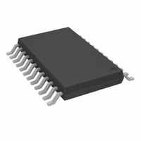
AD8403ARU100-REEL Analog Devices Inc, AD8403ARU100-REEL Datasheet - Page 24

AD8403ARU100-REEL
Manufacturer Part Number
AD8403ARU100-REEL
Description
IC POT DIG QUAD 100K 8B 24TSSOP
Manufacturer
Analog Devices Inc
Datasheet
1.AD8400ARZ1.pdf
(32 pages)
Specifications of AD8403ARU100-REEL
Rohs Status
RoHS non-compliant
Taps
256
Resistance (ohms)
100K
Number Of Circuits
4
Temperature Coefficient
500 ppm/°C Typical
Memory Type
Volatile
Interface
SPI, 3-Wire Serial
Voltage - Supply
2.7 V ~ 5.5 V
Operating Temperature
-40°C ~ 125°C
Mounting Type
Surface Mount
Package / Case
24-TSSOP
Resistance In Ohms
100K
Number Of Elements
4
# Of Taps
256
Resistance (max)
100KOhm
Power Supply Requirement
Single
Interface Type
Serial (3-Wire/SPI)
Single Supply Voltage (typ)
3/5V
Dual Supply Voltage (typ)
Not RequiredV
Single Supply Voltage (min)
2.7V
Single Supply Voltage (max)
5.5V
Dual Supply Voltage (min)
Not RequiredV
Dual Supply Voltage (max)
Not RequiredV
Operating Temp Range
-40C to 125C
Operating Temperature Classification
Automotive
Mounting
Surface Mount
Pin Count
24
Package Type
TSSOP
For Use With
AD8403EVAL - BOARD EVAL FOR AD8403
Lead Free Status / Rohs Status
Not Compliant
Available stocks
Company
Part Number
Manufacturer
Quantity
Price
Company:
Part Number:
AD8403ARU100-REEL
Manufacturer:
A/D
Quantity:
280
Part Number:
AD8403ARU100-REEL
Manufacturer:
ADI/亚德诺
Quantity:
20 000
AD8400/AD8402/AD8403
APPLICATIONS
The digital potentiometer (RDAC) allows many of the applica-
tions of a mechanical potentiometer to be replaced by a solid-
state solution offering compact size and freedom from vibration,
shock, and open contact problems encountered in hostile
environments. A major advantage of the digital potentiometer
is its programmability. Any settings can be saved for later recall
in system memory.
The two major configurations of the RDAC include the
potentiometer divider (basic 3-terminal application) and
the rheostat (2-terminal configuration) connections shown
in Figure 37 and Figure 38.
Certain boundary conditions must be satisfied for proper
AD8400/AD8402/AD8403 operation. First, all analog signals
must remain within the GND to V
single-supply AD8400/AD8402/AD8403. For standard
potentiometer divider applications, the wiper output can be
used directly. For low resistance loads, buffer the wiper with
a suitable rail-to-rail op amp such as the OP291 or the OP279.
Second, for ac signals and bipolar dc adjustment applications,
a virtual ground is generally needed. Whichever method is used
to create the virtual ground, the result must provide the necessary
sink and source current for all connected loads, including
adequate bypass capacitance. Figure 41 shows one channel of
the AD8402 connected in an inverting programmable gain
amplifier circuit. The virtual ground is set at 2.5 V, which allows
the circuit output to span a ±2.5 V range with respect to virtual
ground. The rail-to-rail amplifier capability is necessary for the
widest output swing. As the wiper is adjusted from its midscale
reset position (80
voltage gain of the circuit is increased in successively larger
increments. Alternatively, as the wiper is adjusted toward the B
terminal (code 00
Figure 54 shows the wiper settings for a 100:1 range of voltage
gain (V/V). Note the ±10 dB of pseudologarithmic gain around
0 dB (1 V/V). This circuit is mainly useful for gain adjustments
in the range of 0.14 V/V to 4 V/V; beyond this range the step
sizes become very large, and the resistance of the driving circuit
can become a significant term in the gain equation.
H
H
) toward the A terminal (code FF
), the signal becomes attenuated. The plot in
DD
range used to operate the
H
), the
Rev. E | Page 24 of 32
ACTIVE FILTER
The state variable active filter is one of the standard circuits
used to generate a low-pass, high-pass, or band-pass filter.
The digital potentiometer allows full programmability of the
frequency, gain, and Q of the filter outputs. Figure 55 shows
the filter circuit using a 2.5 V virtual ground, which allows a
±2.5 V
LP, HP, and BP cutoff and center frequencies, respectively.
These variable resistors should be programmed with the same
data (as with ganged potentiometers) to maintain the best
Circuit Q. Figure 56 shows the measured filter response at the
band-pass output as a function of the RDAC2 and RDAC3
settings that produce a range of center frequencies from 2 kHz
to 20 kHz. The filter gain response at the band-pass output is
shown in Figure 57. At a center frequency of 2 kHz, the gain is
adjusted over a −20 dB to +20 dB range determined by RDAC1.
Circuit Q is adjusted by RDAC4. For more detailed reading on
the state variable active filter, see Analog Devices’ application
note AN-318.
V
IN
B
256
224
192
160
128
P
RDAC1
96
64
32
input and output swing. RDAC2 and RDAC3 set the
0
0.1
Figure 55. Programmable State Variable Active Filter
Figure 54. Inverting Programmable Gain Plot
A1
RDAC4
B
OP279 × 2
10kΩ
A2
INVERTING GAIN (V/V)
RDAC2
10kΩ
B
1
0.01μF
A3
RDAC3
B
0.01μF
A4
10
LOW-
PASS
BAND-
PASS
HIGH-
PASS


